Organic Photovoltaic Materials and Devices
Rajiv Giridharagopal, Guozheng Shao, Chris Groves, and David S. Ginger Department of Chemistry, University of Washington, Seattle, WA 98195, USA
Abstract
Organic solar cells hold promise as an economical means of harvesting solar energy due to their ease of production and processing. However, the efficiency of such organic photovoltaic (OPV) devices is currently below that required for widespread adoption. The efficiency of an OPV is inextricably linked to its nanoscale morphology. High-resolution metrology can play a key role in the discovery and optimization of new organic semiconductors in the lab, as well as assist the transition of OPVs from the lab to mass production. We review the instrumental issues associated with the application of scanning probe microscopy techniques such as photoconductive atomic force microscopy and time-resolved electrostatic force microscopy that have been shown to be useful in the study of nanostructured organic solar cells. These techniques offer unique insight into the underlying heterogeneity of OPV devices and provide a nanoscale basis for understanding how morphology directly affects OPV operation. Finally, we discuss opportunities for further improvements in scanning probe microscopy to contribute to OPV development. All measurements and imaging discussed in this application note were performed with an Asylum Research MFP-3D-BIO™ Atomic Force Microscope.
Introduction
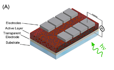
OPV materials are an emerging alternative technology for converting sunlight into electricity. OPVs are potentially very inexpensive to process, highly scalable in terms of manufacturing, and compatible with mechanically flexible substrates. In an OPV device, semiconducting polymers or small organic molecules are used to accomplish the functions of collecting solar photons, converting the photons to electrical charges, and transporting the charges to an external circuit as a useable current.1-3
At present, the most intensely-studied and highest-performing OPV systems are those that employ bulk heterojunction (or BHJ) blends as the active layer, with NREL-certified power conversion efficiencies improving seemingly monthly, and currently standing at 6.77%.4 In a bulk heterojunction blend, the donor and acceptor material are typically mixed in solution, and the mixture is then coated on the substrate to form the active layer. The donor/acceptor pair can consist of two different conjugated polymers, but it is often a conjugated polymer (donor) and a soluble fullerene derivative (acceptor).


