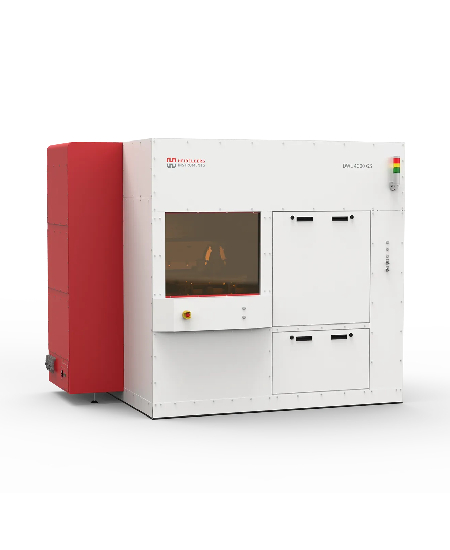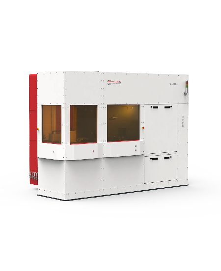
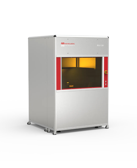
Description
The MLA 150 is an advanced maskless lithography system designed for R&D, rapid prototyping, and low-to-mid-volume production. Using a high-speed Spatial Light Modulator (SLM) and a bi-directional writing process, the MLA 150 eliminates the need for photomasks, significantly reducing cycle times and enabling direct-write lithography with unmatched speed and precision.
Ideal for applications such as nanofabrication of quantum devices, MEMS, micro-optics, sensors, and life sciences, the MLA 150 ensures high-resolution patterning, alignment accuracy, and fast exposure times.
- Maskless Direct-Write Lithography: No photomask required—faster, cost-effective, and highly flexible.
- Fast & High-Precision Alignment:
- Frontside Alignment: 250 nm accuracy
- Backside Alignment: 1000 nm accuracy
- Alignment Error Compensation: Corrects rotation, offset, scaling, and shearing
- Rapid Exposure Speed: 100 x 100 mm² patterns in <10 minutes, full 150 mm wafer in <16 minutes.
- Grayscale Lithography (Standard): Enables 2.5D structuring for advanced micro-optics and waveguides.
- Multi-Laser Compatibility: Supports diode lasers (375 nm & 405 nm) for exposure across different photoresists.
- User-Friendly Software: Features exposure wizards, automatic labeling, CAD integration, and real-time autofocus.
Why Choose MLA 150?
- Eliminates Photomask Costs: Enables direct-write lithography, reducing costs & production time.
- Perfect for Multi-User Research Labs: User-friendly, fast training, and easy operation.
- Optimized for Diverse Applications: Ideal for MEMS, sensors, semiconductor devices, and micro-optics.
- Scalable & Customizable: Flexible exposure area, interchangeable chucks, and multi-laser compatibility.
- Unmatched Speed & Precision: One of the fastest maskless lithography tools available.
- Plug-and-Play Installation: Intuitive workflow and rapid setup for research environments.
Available Modules & Upgrades:
Exposure Wavelength Options:
- Diode Laser Sources: 375 nm and/or 405 nm
- Compatible with all broadband UV photoresists (including SU-8)
Exchangeable Chucks:
- Custom vacuum layouts available for various substrates
Advanced Alignment Features:
- Global & field-by-field alignment
- Alignment error compensation for rotation, offset, scaling, and shearing
Draw Mode:
- Import & overlay BMP files onto a real-time microscope image
- Directly draw simple structures and labels for immediate exposure
Autofocus System:
- Air-gauge or optical autofocus
- Compensation for warped or corrugated substrates
Substrate Size Flexibility:
- Standard: 3” – 6” substrates
- Up to 8” substrates available upon request
Grayscale Lithography:
- 128 grayscale levels for 3D patterning
Click here to view more products from Heildelberg Instruments.
FAQs (Frequently Asked Questions):
What applications is the MLA 150 best suited for?
The MLA 150 is designed for nanofabrication, MEMS, quantum devices, micro-optics, and sensor development.
How does the MLA 150 compare to traditional mask aligners?
It eliminates the need for masks, significantly reducing production time & costs. Any design modification is implemented instantly via CAD software.
How fast is the exposure process?
The MLA 150 can expose a 150 mm wafer in under 16 minutes with a 405 nm laser.
What is the smallest feature size that can be patterned?
The minimum feature size is 0.6 µm, depending on the laser and resist.
Does it support grayscale lithography?
Yes! Grayscale lithography (up to 128 gray levels) is included for 2.5D structuring.
Can it be integrated into a multi-user facility?
Yes! Less than 1-hour training is required for full qualification as a user.
Is the MLA 150 scalable?
Yes! The exposure area is expandable from 150 x 150 mm² to 200 x 200 mm².
What are the laser options?
The MLA 150 supports 375 nm and 405 nm diode lasers, allowing exposure of various photoresists.