Description
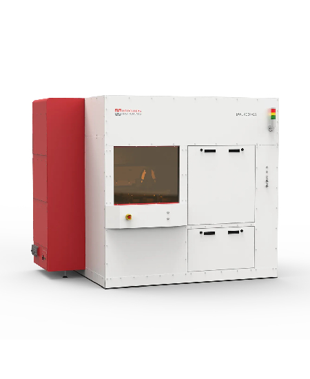
The VPG 300 DI Maskless Direct Imaging System is a high-speed, high-resolution maskless direct imager, engineered for cutting-edge microstructure fabrication. Utilizing a high-power DPSS laser at 355 nm, this system enables sub-micron feature sizes down to 500 nm while providing the flexibility of maskless lithography.
Built for academic research, industrial R&D, and low-volume production, the VPG 300 DI offers precision comparable to a mask-based i-line stepper, but with maskless patterning advantages. It features automated global and local alignment, quasi-stitching-less unlimited die sizes, and distortion correction, making it the ideal solution for MEMS, sensors, semiconductor prototyping, and mixed-signal device fabrication.
Why Choose VPG 300 DI Maskless Direct Imaging System?
- High-Resolution, High-Speed Maskless Lithography: Ideal for MEMS, semiconductor research, sensors, and micro-optics.
- Ultimate Precision for R&D and Prototyping: 500 nm resolution, <40 nm edge roughness, and 100 nm alignment accuracy.
- Cost-Effective & Flexible: No masks required, reducing fabrication costs and enabling on-the-fly design modifications.
- Automated Alignment & Autofocus: VIS/IR alignment, global/local distortion correction, and real-time autofocus.
- Scalable for Various Applications: Works with 100 mm, 150 mm, 200 mm, and 300 mm wafers.
- Quasi-Stitching-Less Patterning: Eliminate alignment errors while creating large-scale structures.
Click here to view more products from Heildelberg Instruments.
FAQs (Frequently Asked Questions):
What applications is the VPG 300 DI best suited for?
The VPG 300 DI is ideal for MEMS, micro-optics, sensor fabrication, semiconductor prototyping, and mixed-signal device lithography.
How does maskless lithography compare to mask-based steppers?
The VPG 300 DI delivers precision comparable to mask-based i-line steppers while offering the flexibility and cost-effectiveness of maskless lithography.
What is the smallest feature size the VPG 300 DI can pattern?
The system achieves feature sizes down to 500 nm with edge roughness of <40 nm.
Does the VPG 300 DI support multi-layer alignment?
Yes! It offers automated global & local alignment with distortion correction and real-time autofocus.
What are the benefits of real-time autofocus?
Autofocus ensures consistent exposure quality, compensating for substrate warping and topographic variations.
Is the VPG 300 DI compatible with automated wafer handling?
Yes! Automated handling for wafers up to 300 mm is available.