Description
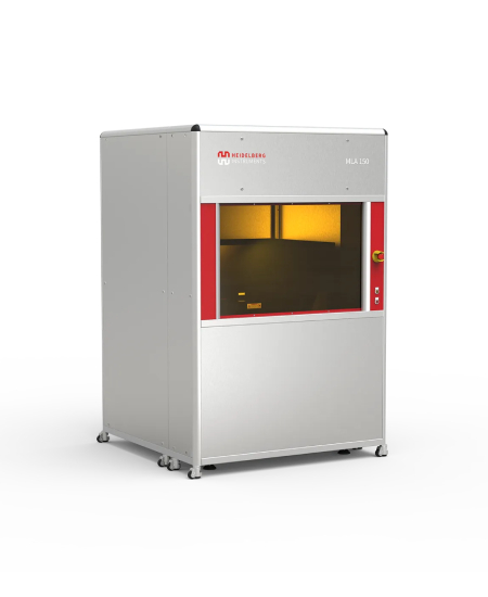
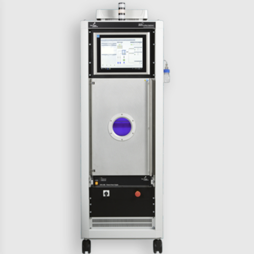
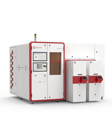
The MLA 300 is an advanced maskless lithography system, engineered for high-throughput industrial manufacturing. It enables direct writing of lithographic patterns without the need for masks, eliminating costly and time-consuming mask production while providing unmatched precision and efficiency.
With real-time autofocus, dynamic distortion correction, and full automation, the MLA 300 seamlessly integrates into manufacturing execution systems (MES), making it the ideal solution for semiconductor fabrication, MEMS, sensors, OLED displays, advanced packaging, and power electronics.
Key Features & Benefits:
High-Speed Maskless Lithography:
- Direct-write exposure eliminates the need for photomasks.
- Faster process adaptation for product customization.
Real-Time Autofocus for Warped Substrates:
- Autofocus compensation range up to 150 µm.
- Critical dimension (CD) uniformity improvement.
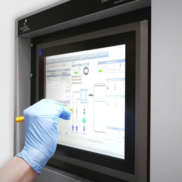
Automated Workflow & Manufacturing Integration:
- Customizable wafer handling options (SEMI-standard cassettes, FOUPs).
- MES integration for automated exposure scheduling.
High-Precision Alignment & Exposure Quality:
- Backside alignment accuracy: 1 µm.
- Second-layer alignment: 500 nm.
Optimized for Cost-Effective, High-Yield Production:
- 10-year laser lifetime reduces maintenance costs.
- No consumables required (compared to traditional mask-based lithography).
Why Choose MLA 300?
- Unparalleled Throughput: 300 x 300 mm² exposure in just 5 minutes (write mode 3, two exposure modules).
- Precise & Scalable: 1.5 µm resolution with automated tracking and overlay correction.
- Eliminates Mask Dependency: Faster product adaptation, reduced costs, and enhanced customization.
- SECS/GEM & OPC-UA Compatibility: Seamless MES integration for Industry 4.0 manufacturing.
- Flexible Substrate Handling: Supports ceramics, warped substrates, and semiconductor wafers.
- Customizable Automation Options: Fully automated substrate handling, backside alignment, and real-time autofocus.
Available Modules & Upgrades:
Automated Wafer Handling:
- SEMI-standard BOLTS plane for FOUP or open cassette integration.
- Custom vacuum chucks for handling warped substrates.
Manufacturing Execution System (MES) Integration:
- SECS/GEM or OPC-UA protocols for automated exposure control.
- Workflow “wizards” for easy operation in production environments.
Backside Alignment:
- VIS or through-wafer IR alignment available.
- 1 µm positioning accuracy for multi-layer lithography.
Multiple Exposure Wavelength Options:
- High-power 7W diode laser (375 nm) for fine-feature lithography.
- 20W diode laser (405 nm) for high-throughput exposure.
Advanced Pattern Correction:
- Per-die corrections for scaling, rotation, and process variations.
- Dynamic compensation for wafer warpage and chip-height variations.
Service Contracts for Maximum Uptime:
- Global service level agreements for fast on-site support.
- Priority access to spare parts and technical expertise.
System Specifications:
| Specification | Write Mode 2 | Write Mode 3 |
|---|---|---|
| Minimum Lines & Spaces | 2 µm | 3 µm |
| Minimum Feature Size | 1.5 µm | 3 µm |
| CD Uniformity (3σ) | 200 nm | 300 nm |
| Edge Roughness (3σ) | 80 nm | 100 nm |
| 2nd Layer Alignment (3σ) | 500 nm | 700 nm |
| Backside Alignment (3σ) | 1000 nm | 1000 nm |
| Max Exposure Speed (405 nm laser) | 9375 mm²/min | 18,000 mm²/min |
| Max Substrate Size | 300 x 300 mm² | 300 x 300 mm² |
| Exposure Time (300 x 300 mm²) | 9.6 min | 5 min |
| Autofocus Dynamic Range | Up to 150 µm | Up to 150 µm |
| Automation & MES Integration | ✅ Yes | ✅ Yes |
Click here to view more products from Heildelberg Instruments.
FAQs (Frequently Asked Questions):
What industries benefit most from the MLA 300?
Semiconductor packaging, MEMS, power electronics, OLED displays, and advanced sensor fabrication.
How does the MLA 300 compare to mask-based lithography?
Maskless lithography eliminates mask costs, reduces turnaround time, and improves production flexibility.
What is the smallest feature size achievable?
1.5 µm in standard write mode and 3 µm in high-throughput mode.
How does the MLA 300 handle warped substrates?
Real-time autofocus and dynamic correction ensure high-quality patterning on non-flat surfaces.
What are the benefits of backside alignment?
It enables precise alignment for double-sided patterning, critical for MEMS and multilayer circuits.
Can the MLA 300 integrate with automated manufacturing workflows?
Yes! It supports SECS/GEM and OPC-UA integration for full MES automation.