You might have seen my previous note [i] about low-current STM imaging of self-assembled 2D lattices of cobalt and nickel octaethylporphyrin (CoOEP and NiOEP, respectively) on HOPG. After seeing the resolution of those images, Roger suggested to me that it might be possible to see the CoOEP lattice using tapping mode AFM (amplitude-modulated AC mode) instead of STM, owing to Cypher’s stability [ii].
“There’s no way that will work,” was Prof. Kerry Hipps’ reply when I relayed that idea. “I’m sure of it.”
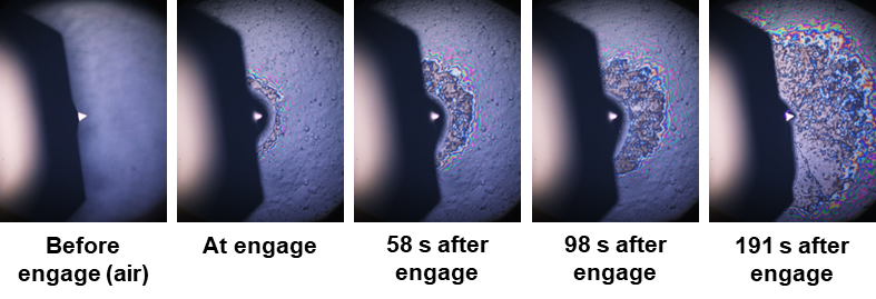
Well, I’m stubborn, so I decided to give it a shot anyway. I chose a FS-1500AuD probe—a sharp, fast, moderately stiff, gold-coated silicon lever (nominally, Rtip = 10 ± 2 nm, fair ≈ 1.5 MHz, k ≈ 6 N/m), which you can find in our probe store. As I engaged the tip to the surface, the thin layer of phenyloctane wicked up onto the probe cantilever (see Figure 1), so the resonant frequency immediately dropped to 0.66 MHz in the now hybrid air-liquid oscillatory medium. It took about 10 minutes for the wicked solution to equilibrate, after which time it was stable even as I moved around the surface.

Figure 1. Time series of images of interference fringes at the phenyloctane/HOPG interface. These images were captured through the Cypher ES topview optics, and the fringes arise from a phenyloctane meniscus acting as a diffractor as the solution wicks up onto the AFM cantilever.
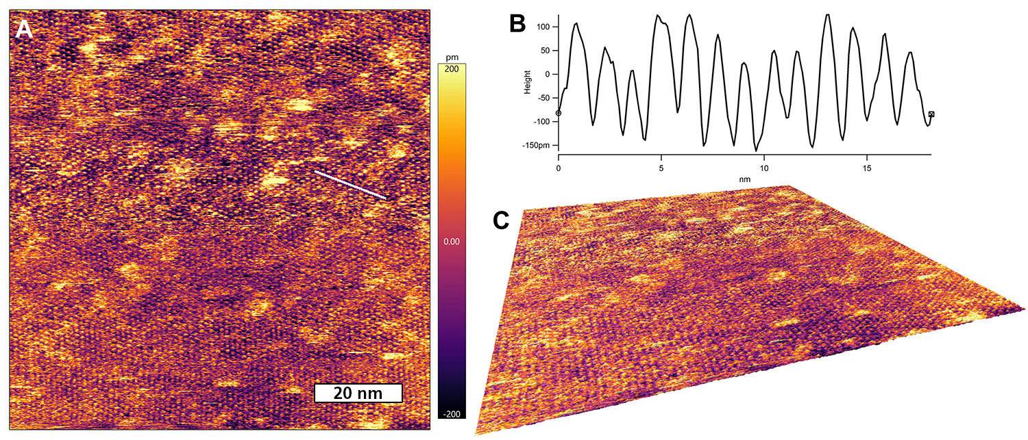
After tuning the cantilever in the equilibrated solution, I was able to maintain a stable free drive amplitude of ~1.44 nm (90 mV) and a setpoint of ~0.34 nm (21 mV), thanks to the exceptional stability of blueDrive photothermal excitation [iii]. Lo and behold, the CoOEP lattice came into view, with the expected molecular spacing of ~1.4 nm! After I showed him the image in Figure 2, all Prof. Hipps had to say was, “Wow.”
Figure 2. Low-amplitude tapping mode molecular lattice resolution of CoOEP.(A) 100 nm survey scan. (B) Line trace along the white line in (A) showing the regular spacing of CoOEP molecules. (C) 3D rendering of the 100 nm image for perspective.
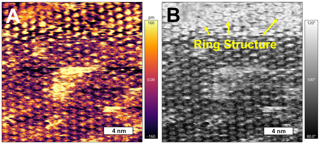
After zooming in (Figure 3), I convinced myself that I could see the porphyrin ring structure in part of the phase image. The thing you might notice here is that the measurements are much more sensitive to contamination than the STM images in the last note. We see some amorphous globs on the surface as well as changes in the image as the scan progresses due to tip-glob interactions. This simply means that you have to be extra-diligent about cleaning your sample, the probe, and the probe holder prior to AFM measurements.
Figure 3. Zoomed in tapping mode AFM images of the CoOEP lattice. (A) Height topography; 20 nm scan. (B) Phase; 20 nm scan. Note the porphyrin ring structure apparent in the upper section of the image.
These data remind me of a few AFM studies [iv-vi] using Cypher in ambient conditions that were published a few years ago by Prof. Rob Atkin (The University of Newcastle), Prof. Peter Beton (University of Nottingham), and Prof. Xinran Wang (Nanjing University). The first study [iv] elucidated the nanostructure of an ionic liquid (EMIm+ TFSI–) under potentiostatically-controlled bias at a graphite (HOPG) surface (see Figure 4A). Further, the applied bias was varied systematically around the open circuit potential, and the molecular Stern layer reorganized as a function of bias (as well as ionic components, such as Li+ and Cl–). The second study [v] looked at the supramolecular organization of 5,10,15,20-tetrakis(4-carboxylphenyl)porphyrin (TCPP) adsorbed on hexagonal boron nitride (hBN) and other surfaces and the effect of that adsorption on the optoelectronic properties of the TCPP molecules. Figure 4B shows the square lattice structure of TCPP on hBN. The third study [vi] explored van der Waals epitaxy of few-layer 2D molecular crystals of high-mobility dioctylbenzothienobenzothiophene (C8-BTBT) on HOPG and hBN for applications in organic field-effect transistors. Figure 4C shows the high-resolution topography of the lattice of C8-BTBT grown on hBN.
Figure 4. Previous AFM imaging of 2D molecular lattices. (A) Phase image of a pure EMIm+ TFSI– Stern layer adsorbed to a HOPG substrate; 30 nm scan, imaged in the bulk EMIm+ TFSI– ionic liquid (see Ref. [iv]). (B) Height image of the square lattice of TCPP assembled on hBN substrate; 50 nm scan, imaged in air (see Ref. [v]). (C)Height image of the lattice of C8-BTBT grown on hBN substrate; 10 nm scan, imaged in air (see Ref. [vi]).
For imaging ionic liquids, STM has been the standard analytical technique. AFM has revealed new detail about their interfacial structures, largely because as an ambient technique it avoids the conventional artifacts that are induced by freezing monolayers of an ionic liquid under ultra-high vacuum. STM is also only possible with conductive samples (which many materials are not), so high-resolution AFM allows for a new avenue of characterization for interesting semiconductor and insulator nanomaterials. Gone are the days when sub-nanometer molecular resolution was the province of only STM. It is clear that next-generation AFMs like Cypher are readily reaching into that resolution realm, revealing nanoscale features that before might not have even been observable with STM.
References
[i] April Current Amplifiers Bring May Ultra-Low-Current STM
[ii] Learn more about Cypher here: https://www.oxford-instruments.com/products/atomic-force-microscopy-systems-afm/asylum-research/high-resolution-fast-scanning-afm.
[iii] (a) Learn more about blueDrive at https://afm.oxinst.com/bluedrive and at https://pdfs.semanticscholar.org/e807/9171fb282e6340f6813a0f6b8cee8b4bae74.pdf. (b) A. Labuda, K. Kobayashi, Y. Miyahara, and P. Grütter, Retrofitting an atomic force microscope with photothermal excitation for a clean cantilever response in low Q environments, Review of Scientific Instruments, 2012 83, 053703. https://aip.scitation.org/doi/abs/10.1063/1.4712286.
[iv] A. Elbourne, S. McDonald, K. Voïchovsky, F. Endres, G. G. Warr, and R. Atkin, Nanostructure of the Ionic Liquid–Graphite Stern Layer, ACS Nano, 2015, 9(7), 7608–7620. https://pubs.acs.org/doi/abs/10.1021/acsnano.5b02921.
[v] V. V. Korolkov, S. A. Svatek, A. Summerfield, J. Kerfoot, L. Yang, T. Taniguchi, K. Watanabe, N. R. Champness, N. A. Besley, and P. H. Beton, van der Waals-Induced Chromatic Shifts in Hydrogen-Bonded Two-Dimensional Porphyrin Arrays on Boron Nitride, ACS Nano, 2015, 9(10), 10347–10355. https://pubs.acs.org/doi/10.1021/acsnano.5b04443.
[vi] D. He, Y. Zhang, Q. Wu, R. Xu, H. Nan, J. Liu, J. Yao, Z. Wang, S. Yuan, Y. Li, Y. Shi, J. Wang, Z. Ni, L. He, F. Miao, F. Song, H. Xu, K. Watanabe, T. Taniguchi, J.-B. Xu & X. Wang, Two-dimensional quasi-freestanding molecular crystals for high-performance organic field-effect transistors, Nature Communications, 2014, 5:5162, 1–7. https://www.nature.com/articles/ncomms6162.


