Material Surface Characterization Made Easy With Tensiometry and Optical Profilometry – SRC Seminars and Workshops Series – Toronto Metropolitan University

Join us for an enlightening day of cutting-edge insights into Material Characterization and Surface Science, hosted in collaboration with our trusted partners Biolin Scientific and Sensofar. This workshop is an invaluable opportunity to delve into the latest advancements in analytical instruments, discover their real-world applications, and network with industry experts.

Date: November 29th, 2023
Time: 8:30 AM – 4:30 PM
Location: Room HEI 101
Address: 125 Bond St, Toronto, ONM5B 1Y2

Event Agenda and Details:


Register Here:

Material Surface Characterization With Tensiometry and Optical Profilometry

Join us for an enlightening day of cutting-edge insights into Material Characterization and Surface Science, hosted in collaboration with our trusted partners Biolin Scientific and Sensofar. This workshop is an invaluable opportunity to delve into the latest advancements in analytical instruments, discover their real-world applications, and network with industry experts.

Date: November 27th, 2023
Time: 8:30 AM – 4:30 PM
Location: Genomics Building (GE), Room GE 110.00, Concordia University, Loyola Campus, Montreal. Click Here for the Maps

Event Agenda and Details:


Got Questions?

XPS Surface Analysis for Battery Research

What is XPS?

X-ray photoelectron spectroscopy (XPS) is a powerful surface analysis technique used to identify the elements in and the chemical states of the top layers of materials. It works by bombarding the surface of a material with X-rays (photons) and then measuring the kinetic energy of the photoelectrons ejected from the surface of a material. This energy is directly related to the photoelectrons’ binding energy within the parent atom and is characteristic of the element and its chemical state. Only electrons generated near the surface can escape without losing too much energy for detection. As a result, XPS data is obtained only from the top few nanometers of the surface. XPS surface selectivity, combined with quantitative chemical state identification, makes XPS highly useful in many applications, including battery research.

Vital role of battery research

Batteries have a vital role to play in the world’s transition from fossil fuels to renewable energy. In 2022, EVs accounted for 10% of global vehicle sales and by 2030 they are expected to reach 30% of global vehicle sales.  Governments around the world are contributing to this growth through policies that are directing billions of dollars into battery research and manufacturing and by providing subsidies for consumers to purchase EVs.  Ambitious cost and performance targets for the electrification of transportation will require the development of next-generation batteries produced on a commercial that are cost-effective, safe, renewably sourced, and high-performing with long lifetimes.

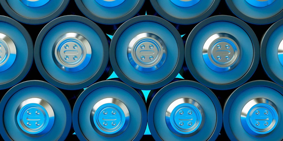
Cells in Battery

How XPS is used in battery research

There are multiple components and interfaces that are crucial to understand to develop high-performing and stable batteries. These include the cathode, anode, separator, electrolyte, and all interfaces formed between these layers, particularly the electrode-electrolyte interfaces. XPS can be used to study all of these materials and interfaces, such as next-generation cathode/anode active materials and how their composition changes with cycling; how the solid electrolyte interphase (SEI) layer varies in composition as a function of depth; and how surface pre-treatments affect the chemistry of the active electrode material. The quantitative chemical-state information provided by XPS makes it a versatile tool to understand many properties and guide the design of optimized batteries that meet ambitious targets.

Battery research challenges and XPS solutions:

  • Analyzing SEI layer growth: Ongoing charging and discharging of a battery causes the SEI layer to form on the anode, reducing battery capacity. Analysis of the SEI layer helps researchers better understand and control this phenomenon and thereby improve battery performance and longevity. XPS depth profiling can chemically characterize the complex mixture that makes up the SEI layer, from the anode side all the way to the electrolyte side, for chemical understanding of the entire layer.
  • Investigating the role of impurities and contaminants: Impurities and contaminants in battery materials can adversely affect performance and safety. XPS is highly sensitive to trace elements and can identify the presence and identity ofimpurities or contaminants on the surfaces of battery materials, helping researchers understand the sources of impurities and their impact on battery performance.
  • Understanding the stoichiometry of solid electrolyte films: Chemical state analysis provided by XPS can be used to identify the stoichiometry of materials, including depth profiling to quantify elements at each depth and track any differences in stoichiometry throughout a film.
  • Studying interface chemistry: Interfaces between different components of a battery play a crucial role in battery performance and long-term stability. XPS provides insights into the chemistry of interfaces, helping researchers optimize interface design for enhanced performance.
  • Examining degradation in separator chemistry: XPS can provide valuable insights into degradation in separator chemistry during a cell’s lifetime by analyzing the surface chemistry and composition of the separator material.
  • Environmental impact and recycling: XPS can be used to analyze the chemical composition of battery materials before and after recycling processes. It can help assess the effectiveness of recycling methods and the feasibility of reusing materials.
  • Analyzing in situ electrode cycling: In situ XPS experiments can provide real-time insights into the electrochemical behavior and surface chemistry of electrode materials during cycling.

The best XPS for battery research from SRC

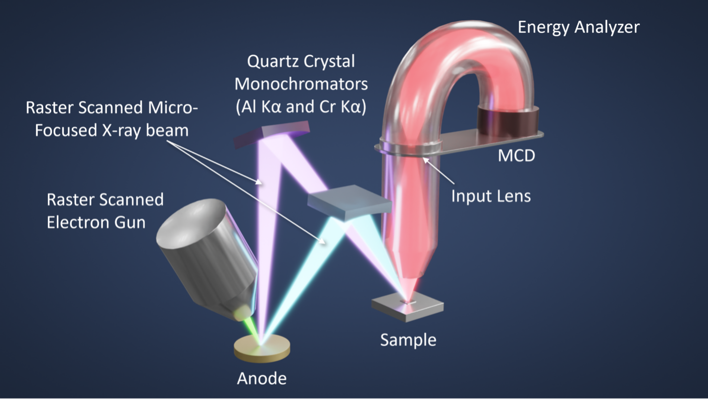
PHI’s XPS instruments use a unique scanned, finely-focused X-ray beam to create X-ray induced secondary electron images (SXIs), similar to an SEM, for easy sample navigation with 100% certainty in analysis position.  This imaging capability can be used to easily drive around the sample in live mode or to save positions for compositional analysis including point or large-area spectroscopy, line scans, depth profiling, or chemical mapping. The size of the X-ray beam can be selected to support the efficient analysis of larger samples with homogeneous composition or small heterogeneities. This feature is indispensable for analyzing battery materials and interfaces, ensuring identification of impurities or other heterogeneities in composition, and absolute certainty that data is acquired from the exact feature of interest. In contrast to SEM/EDS, which has a typical analysis depth of 1-3 µm, XPS is a surface-sensitive technique with a typical analysis depth of less than 5 nm, making it better suited for the compositional analysis of ultra-thin layers and thin microscale sample features.

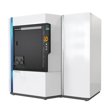
phi genesis Product Image Genesis Geometry Schematic

The PHI Genesis is the latest generation of PHI’s highly successful multi-technique XPS product line with PHI’s patented, monochromatic, micro-focused, scanning X-ray source. It is an easy-to-use, fully automated system with auto-tuning and calibration and multiple parking positions for high throughput. The fully integrated multi-technique platform of the PHI Genesis offers an array of optional excitation sources, sputter ion sources, and sample treatment and transfer capabilities that are all aligned to the same sample location. These features are essential in studying all relevant properties of advanced battery materials and interfaces, including small impurities or compositional heterogeneities, access to buried interfaces, electronic energy gap measurements, and operando experiments for a direct link between chemistry and performance. PHI Genesis offers high sensitivity and high throughput for large areas and small areas down to 5 µm and unique high-throughput non-destructive depth profiling using the optional hard X-ray Cr source. The instrument is fully customizable to address all analytical needs.

For more information on how PHI Genesis can be used to address your battery characterization challenges, please visit the PHI YouTube channel to watch a recent PHI.


Contact Us:

Click here to contact SRC and speak directly with experts on PHI’s Genesis.

New Product Announcement: The New PHI Genesis

phi genesis with Spectra Research Corporation

The New PHI Genesis

XPS and HAXPES combined in an automated multi-technology platform

SRC is pleased to announce the release in Canada of the new PHI Genesis from Physical Electronics. The new PHI Genesis—the latest generation of ULVAC-PHI’s highly successful multi-technique XPS product line—eliminates the need to compromise by combining PHI’s successful scanning XPS/HAXPES microprobe product lines into a single, compact instrument. This delivers the VersaProbe’s multi-technique capabilities with the Quantes/Quantera’s high throughput automated analysis. The new PHI Genesis represents a real breakthrough in XPS analysis.

Market for the PHI Genesis

A broad range of high-tech products are made of complex combinations of advanced materials designed to deliver superior performance across a range of metrics. R&D of these complex combinations of materials requires rapid optimization of the performance of each material, as well as the combinations of materials. There is a growing need for powerful and highly functional surface and interface analysis that can significantly accelerate this work.

XPS and HAXPES generate vital information that provides insights into the properties and behaviour of advanced materials. Other key tasks that XPS and HAXPES can deliver on include defect analysis and the testing of cleaning processes. XPS has an information depth of about 5nm while HAXPES has an information depth of about 15nm. Click Here to learn more.


New PHI Genesis areas of application

  • Semiconductors
  • Batteries
  • Organic devices
  • Catalysts
  • Quantum dots
  • Nanoparticles
  • Bio and life science materials
  • Polymers
  • Ceramics
  • Metals
  • Other solid materials and devices

Advantages of the new PHI Genesis

  • Simple, intuitive and easy-to-use user interface experience
  • With powerful XPS, HAXPES, UPS, LEIPS, REELS, AES and a variety of other options, it meets all your surface analysis needs
  • The unsurpassed 5 µm X-ray beam with a small spot opens up new possibilities for micro-XPS applications
  • High-throughput, high-performance depth profiling
  • Non-destructive depth profiling, sputter-free depth probing using a high-energy hard X-ray source that generates information from a greater depth than with conventional soft X-ray XPS

About Physical Electronics

Physical Electronics is a subsidiary of ULVAC-PHI, the world’s leading supplier of UHV surface analysis instrumentation used for the research and development of advanced materials. Fields of application for their products include: nanotechnology, microelectronics, photovoltaics, data storage, bio-materials and catalysis. PHI’s innovative XPS, AES and TOF-SIMS technologies provide customers with unique tools to solve challenging materials problems and accelerate the development of new materials and products. For more information on this product please click here.

Sensofar Event 22 – New Integrable Heads launch

We’d love to see you at Sensofar Event 22!

We believe that the future is built by listening to the needs of our users, as well as the market, to constantly improve what we do.
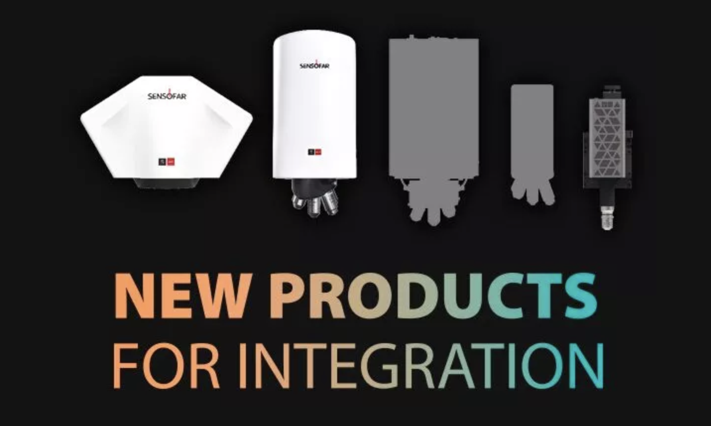
We have spent a while working on two new products for you, and they are finally ready to unveil at Sensofar Event 22:
the S mart 2 and the S neox Cleanroom.

We prepared an incredible event to show you the two new heads from our integration line! It will take place on November 16 in a completely virtual format to make it as easy as possible for you all to attend. It will be the perfect opportunity to hear first-hand all their technical features and capabilities.

Event Speakers

Understanding and Using High Magnification Inspection

September 28 @ 12:00 pm1:00 pm

Join CCAT and Sensofar for a free webinar about high magnification inspection of critical dimensions as well as surface finishes for additive manufacturing, medical devices, tribology and tooling applications.

We’ll explore the technology used for surface roughness measurements and dimensional measurements and also present solutions for key applications in aerospace and advanced manufacturing using optical metrology.

Target Audience
Metrology and Inspection, Aerospace and Additive Manufacturing Engineers 

Presenters
Adam Platteis, Sales Manager USA, Sensofar
David Morganson, Manufacturing Applications Engineer, CCAT

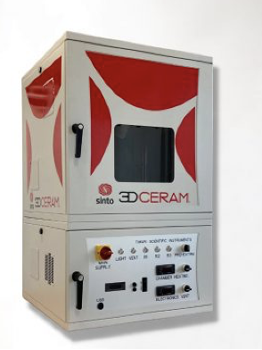
New Product: Raptor 3D Printer from 3DCeram Sinto Tiwari

Sinto Tiwari


Spectra Research Corporation (S.R.C.) is pleased to announce a new product offering, Raptor 3D Printer for Fused Filament Fabrication (F.F.F.) 3D printing for metals and ceramics. Earlier this year, Ceramic S.L.A. market leader 3DCeram Sinto became a significant shareholder of Tiwari Scientific Instruments, a German space and industrial research start-up. This acquisition led to their rebranding as 3DCeram Sinto Tiwari.
Raptor 3D

The Raptor 3D Printer, supplied by 3DCeram Sinto Tiwari, is suitable for the cost-effective production of ceramic and metal parts using F.F.F. The process uses specially fabricated bound metal or ceramic filaments shaped into your desired geometry. The printed parts may then be machined to include further details and improve the finish. They can then be heat-treated at high temperatures to eliminate the binder and sintered parts. The Raptor 3D printer yields metal and ceramic parts with a relative density of over 99%.

3DCeram Sinto Tiwari’s printers currently support metals including Copper, Stainless Steel (316L & 17-4PH), and Titanium (Ti6Al4V). The ceramics they support include Alumina (Al2O3), Silicon Carbide (SiC), Silicon Nitride (Si3N4), Tungsten Carbide-Cobalt (WC-Co), Zirconia (ZrO2) and Molybdenum disilicide (MoSi2).

This new acquisition aims for 3DCeram Sinto to offer to integrate the F.F.F. technology into their operations to work with some of the most advanced ceramic and metal materials. The purchase is part of a Sinto group development program titled Multi Advanced Technologies (M.A.T.), which intends to provide a new type of additive and intelligent manufacturing organized in digital networks. The program aims to respond to the imperatives of ecology, sustainable development, and precision by offering a new way of considering the production of parts. 

Contact Us

S.R.C. continues to offer our customers a range of innovative, high-quality scientific products and laboratory services throughout Canada for industrial and scientific markets. For more information about 3DCeram Sinto Tiwari or using their Raptor 3D Printer for metal and ceramics fabrication in manufacturing or R&D, please contact a member of our staff.

New Product: Heidelberg Instruments’ MPO 100

Spectra Research Corporation (SRC) is pleased to announce a new product offering, MPO 100, A multi-user tool for 3D Lithography and 3D Microprinting from Heidelberg instruments.


Heidelberg instruments, an SRC supplier, is headquartered in Germany. They have been a world leader in developing and producing high-precision photolithography systems, maskless aligners, and nanofabrication tools for over 35 years. The MPO 100 is a Two-Photo Polymerization (TPP) multi-user tool for 3D Lithography and 3D Microprinting of microstructures with applications in Optics, Photonics, Mechanics, and Biomedical Engineering. It includes a powerful femtosecond laser system operating at a wavelength of 266nm, enabling efficient and high-speed processing of many commercially available systems. As many photoresists exhibit high sensitivity at the 266nm TPP wavelength, the MPO 100 is an ideal tool for research and development to produce new material systems.
SRC | 3D Lithography and Micro-Printing
Unique features of the MPO 100:
  • Printing height of over 1cm
  • Surface quality: smooth surfaces down to 10nm
  • High resolutions print: features sizes smaller than 100 nm
  • High-speed 3D microfabrication: Scan Speeds over 1000 mm/s
  • Temperature-controlled flow box to ± 0.1 °C with ISO4 environment
  • Application-specific write modes enable fast and easy switching between 3D Lithography and 3D Microprinting.
  • A synchronized scanning system enables stitching-free fabrication
  • Various exposure and write modes tailored to the specific applications
  • High-speed processing of ORMOCER®s (hybrid polymers) and other photoresists

The MPO 100 includes a powerful femtosecond laser system operating at a wavelength of 266 nm, enabling efficient and high-speed processing of many commercially available polymer systems.

The scanning system of the MPO 100 consists of high-performance, frictionless air-bearing stages synchronized with the high-speed galvo scanner. This enables a simultaneous movement of the sample and a deflection of the laser spot, thereby expanding the scan field (Field-of-View, FoV) of the microscope objective to the entire print area of 100 mm x 100 mm and thus providing the capability of stitching-free fabrication (infinite FoV).

Software

The MPO 100 includes the software package of LithoStream and LithoSoft3D as standard.

LithoStream is the MPO 100 control software. It provides unique features like printing time estimation, triangulation, process camera, alignment, print job creator, and application programming interface (API). Printing parameters can be saved into a database, and printing recipes can be loaded.

LithoSoft3D is code preparation software. It includes powerful modules to handle and process application-specific design formats such as stl- or bitmap files with advanced stitching options. Depending on the user‘s requirements, different trajectory models can be chosen, like a full volume scan, contour scan, or the combined contour hatch scan, as well as the LCON3D (real 3D Laser CONtouring).

About Heidelberg Instruments

Having over 35 years of experience and more than 1,200 systems installed worldwide, Heidelberg Instruments provides lithography solutions specifically tailored to meet all your micro- and Nanofabrication requirements, no matter how challenging.

To remain at the forefront of their industry, they continuously expand their vast knowledge in Micro- and Nanofabrication and work to advance their specialized engineering skills in mechanics, electronics, optics, and software. This combined unique expertise enables them to develop exclusive solutions that outperform conventional lithography machinery and empower customers.

Contact

SRC continues to offer our customers a range of innovative, high-quality scientific products and laboratory services for industrial and scientific marketing throughout Canada. For more information about the MPO 100 and how it can best serve your goals, we encourage you to reach out to a member of our staff.