PHI Webinar Series: TOF-SIMS 101: Introduction, Ion Beams, MS/MS, and Materials Applications

PHI Webinar
PHI Webinar

 PHI WEBINAR SERIES: 

TOF-SIMS 101:

Introduction, Ion Beams, MS/MS, and Materials Applications


FREE LIVE WEBINAR 

Thursday, May 14, 2020 – 10:00am (Chicago)

Time-of-Flight Secondary Ion Mass Spectrometry (TOF-SIMS) is a powerful analytical technique that can provide elemental and molecular information with high sensitivity from the sample surface to tens of microns into the sample. Additionally, TOF-SIMS can produce chemical images with high spatial resolution (<70 nm). This is achieved by utilizing a variety of ion beams to either analyze (Binq+, Au nq+, C60q+, Ga+), sputter (O2+, Cs+, Ar+, large gas cluster Ar), or mill (Ga+ FIB) the sample. The most recent advancement in TOF-SIMS is the capability of MS/MS (i.e. tandem MS) which enables confident molecular identification. The flexibility of TOF-SIMS makes it a valuable tool to investigate a wide range of materials. This webinar will introduce the fundamentals of TOF-SIMS, discuss ion beams and MS/MS, and show materials applications.


WHEN

  • Thursday, May 14, 2020 – 10:00am (Chicago)

WHAT

  • TOF-SIMS 101: Introduction, Ion Beams, MS/MS, and Materials Applications

PRESENTER

  • Andrew Giordani – Physical Electronics Staff Scientist

PLEASE CLICK THE LINK BELOW TO REGISTER FOR THE EVENT!

Sensofar Metrology

Sensofar Metrology

Sensofar Metrology is one of two divisions of the Sensofar group, based in Barcelona, Spain, an innovation and technology hub. Sensofar Metrology is renowned for its:

  • High-end, non-contact, 3D surface profilers based on complementary confocal, interferometry, focus variation and spectroscopy reflectometer techniques;
  • Consultancy within the field of metrology;
  • Advanced R&D generating patented technologies contributing to hundreds of surface metrology applications worldwide.

Non-contact 3D surface metrology

3D surface metrology is the measurement and characterization of micro- and nano-scale features on natural or manufactured surfaces. This is done efficiently by capturing the 3D spatial coordinates of points on a surface using a non-destructive optical technique.

Sensofar

 Surface topography at the nanometer level

Optical surface profilers have crucial advantages over tactile approaches:

  • Measurement is non-contact, so there’s no damage to the object being measured;
  • Optical techniques can measure through transparent media, are fast and flexible, and yield 3D (areal) results;
  • Measurement performance depends on wavelength and numerical aperture, eliminating limitations caused by the physical size of a stylus tip.

The most common optical techniques available are confocal, interferometry and focus variation, each of these has their own strengths and weaknesses.

Sensofar Metrology_2.png

Superior vertical resolution with confocal

Confocal: Confocal profilers measure the surface height of smooth to very rough surfaces, with spatial sampling as low as 0.10 μm—ideal for critical dimension measurements. High NA (0.95) and high magnification (150X) objectives are available to measure steep local slopes >70° on smooth surfaces with and up to 86° on rough surfaces. Sensofar’s proprietary confocal algorithms provide vertical repeatability on the nm scale.

Interferometry: White-light vertical scanning interferometers (VSI) measure the surface height of smooth to moderately rough surfaces, providing nm vertical resolution regardless of the NA. Sensofar’s new S neox optical 3D profiling microscope can use all available magnifications to profile shape features with no compromise in height resolution.

Focus variation: Focus variation has been developed for measuring the shape of large rough surfaces. Sensofar’s implementation of this approach has been specifically designed to complement confocal measurements at low magnification. Highlights of the technology include high slope surfaces (up to 86°), highest measurement speeds (mm/s) and large vertical range. This combination of features is largely suited to tooling applications.


Sensofar Metrology products

New S neox: The new S neox optical 3D profiling microscope outperforms all previous microscopes of its kind in terms of performance, functionality, efficiency and design. It combines all three of the above techniques: confocal (best for surfaces with high slopes), interferometry (highest vertical resolution) and focus variation (measures shape in seconds). The S neox does all this in the same sensor head without any moving parts. The S neox delivers three-in-one technologies for class-leading areal measurement.

Sensofar Metrology_4.png

S neox helps in archaeological study of an ancient rock drawing

S neox Five Axis: The S neox Five Axis S measures samples at different positions of rotation and elevation,thereby generating a group of individual measurements. The SensoFIVE software merges all of the surfaces, providing a sample surface with high accuracy by using the stacked image information of each single surface measurement. Merging different elevations, the system can provide shape and form information on sharp edges and/or critical surfaces.

Request a quote

Click here to request a quote on any Sensofar product.

Workshop : Hybrid Nano-lithography Technology combining Thermal SPM and Direct Laser Lithography

Hybrid Nano-lithography Technology_1

SwissLitho commercialized tSPL

This fall SwissLitho is releasing its newest product “NanoFrazor Explore DLS“. This unique hybrid nano-micro lithography system, which combines thermal Scanning Probe Lithography (tSPL) with Direct Laser Sublimation (DLS) was developed by Heidelberg Instruments and SwissLitho.

SwissLitho commercialized tSPL out of IBM Research in 2014 and its commercial NanoFrazor systems are installed at various institutions and used for the fabrication of nanodevices when usual nanolithography techniques get complicated or fail.

You are cordially invited to this workshop which aims to introduce the capabilities of the technologies of Heidelberg Instruments and SwissLitho and discuss their opportunities for McGill University researchers.

Date and time: 1:30 pm, Sept 17th, 2019

Place/Room: Rutherford Physics building, RM 105, 3600 University street


Program:
1:30 pm NanoFrazor lithography – an overview
1:55 pm
NanoFrazor DLS – mix&match lithography in the same resist and same system
2:20 pm
Overview on various pattern transfer processes for NanoFrazor lithography
2:45-3:00 pm
Open user discussion
3:00-5:00 pm
Live System demo in CR

SRC logoWe are looking forward to seeing you at our workshop!

For more information please contact : Serge Dandache
Hybrid Nano-lithography


lithography Technology

New Generation Theta Optical Tensiometer from Biolin Scientific

Optical tensiometer; Smart interfacial measurement solutions for wettability and adhesion

The new generation Theta Optical Tensiometer (Attension® Theta Flex) from Biolin Scientific  is a contact angle meter that enables all measurements in one instrument for both research and quality control. It measures static and dynamic contact angle, 3D surface roughness, surface free energy, surface and interfacial tension, and interfacial rheology.

Theta Optical Tensiometer

One instrument for all your measurement needs

All the measurements are readily included in the software. Thanks to the modular design, all applications can be fulfilled with one instrument and the instrument can be tailored for your needs.

Results you can rely on

High-end imaging together with sophisticated analysis algorithms detect and analyze the contact angle and surface free energy precisely. The effect of roughness to wettability can be measured with the unique 3D Topography module.

Speed and repeatability

All steps from loading the measurement to performing it and analyzing the data can be automated. The need for time consuming preparations and cleaning are removed with the disposable liquid tips.

Applications

Optical tensiometers are used in a great variety of industries and research areas, such as chemicalspharmaceuticalselectronicsfoodsenergypaper and packaging. Attension Theta Flex can be used for convenient and precise studies of:

  • Wettability
  • Adhesion
  • Homogeneity
  • Surface roughness
  • Spreading
  • Cleanliness
  • Printability
  • Adsorption
  • Emulsion and foam stability

Measurements

Attension Theta Flex can perform a complete range of measurements including:

  • Static contact angle with the sessile drop, captive bubble and meniscus methods
  • Dynamic contact angle with the tilted drop and sessile drop methods
  • Surface free energy with the sessile drop, captive bubble and meniscus methods
  • Surface- and interfacial tension with the pendant drop and reverse pendant drop methods
  • Roughness-corrected contact angle and 3D surface roughness with the Fringe projection phase shifting method
  • Interfacial dilatational rheology with the pulsating drop method

OneAttension software

OneAttension features an intuitive user interface, live analysis and configurable user groups and accounts. In-depth analysis of your results takes a few seconds and data can easily be exported.

Modules and accessories

Attension Theta Flex enables you to choose the level of automation and the advanced functionalities that you need for your applications. With the modular design and an extensive range of modules and accessories you have room to upgrade or change the instrument as your needs evolve.

Attension Theta Flex: one instrument for all your measurement needs.

For more information or to request a quote, please contact us.

Herzan Happenings – Fall 2018 Edition

Herzan_1

Herzan_2.png

This exclusive quarterly newsletter highlights the latest product announcements, application specific solutions, and news about the company. Take a look inside the latest developments at Herzan and see if these new developments can complement your research!

IN THIS ISSUE

Stop By Booth 809 at the MRS Fall Meeting in Boston, MA

Save Big On Herzan’s Most Popular Products During Fall Savings Program

Featured Case Study: SEM Improves Stability Using Herzan’s AVI Platform

Herzan Happenings - Fall 2018 Edition

Herzan Happenings – Fall 2018 Edition

B&W Tek November Newsletter

Advances in Raman throughout the Pharmaceutical Manufacturing Process 

The importance of quality control in continuous manufacturing has lead to a rapid increase in the use of Raman spectroscopy. In our latest webinar we explore how Raman spectroscopy is paving the way for innovation in advanced manufacturing techniques, with a presentation by Dr. Douglas Hausner of Associate Director of Rutgers University’s  Engineering Research Center for Structured Organic Particulate Systems (C-SOPS).

New E-Book on the Tools, Techniques and Applications of Raman Spectroscopy

Portable and handheld Raman systems are gradually replacing slow and destructive techniques that have been widely used throughout the pharmaceutical industry. This month, B&W Tek partnered with American Pharmaceutical Review to release a new E-Book highlighting these recent developments in the industry. The E-book features various tools, techniques and applications that use Raman Spectroscopy to perform tasks such as at-line content uniformity, counterfeit detection and raw material identification.

Meet the Team!

Meet Kevin Wu: a seasoned foodie, full time cat dad and the new inside sales administrator at B&W Tek! Kevin is a Delaware native who graduated from Drexel University with a degree in criminal justice. He now uses his 7 years of experience in aviation quality control to give clerical assistance to our account managers and handle logistics for our sales team. It would be an understatement to say that we are excited to have Kevin join the B&W Tek family!

View our upcoming events!

California Narcotics Officers Assocation Training Expo
Booth 212
San Diego, California

November 16-20, 2018

MRS Fall 
Booth 611
Boston, Massachusetts
November 25-30, 2018

USBTA Technology Training Expo
Technology Training Lane
Orlando, Florida

December 2-4, 2018


AVS 65 Lunch n Learn – Complementary XPS & TOF-SIMS

AVS 65 Lunch n Learn Complementary XPS TOF-SIMS

Physical Electronics User Reception

AVS 65 – Long Beach, CA

Physical Electronics would like to cordially invite you to join us on
Monday, October 22, 2018 from 8:30-10:30pm at the Hyatt Regency Long Beach in the Beacon Ballroom (Sec. A) for appetizers and drinks
for our annual PHI User Reception. 

WHEN: Monday, October 22, 2018, 8:30-10:30pm(Immediately following Welcome Mixer)
WHERE: Hyatt Regency Long Beach – Beacon Ballroom (Sec. A)
Drinks and Appetizers will be provided.

Please RSVP for the reception by emailing Ben Ellefson 
at  Bellefson@phi.com  by October 19 if you’ll be able to attend. 

For the characterization of polymers and organic-coated surfaces, the combination of two surface sensitive techniques – X-ray Photoelectron Spectroscopy (XPS) and Time-of-Flight Secondary Ion Mass Spectrometry (TOF-SIMS) can be extremely powerful.  XPS provides quantitative analysis and short-range bonding chemistry from elements on the outermost surface while TOF-SIMS can provide the molecular information needed to positively identify organic species and the spatial resolution needed to show their lateral distributions on the sample surface.  This presentation will discuss the complementary attributes of XPS and TOF-SIMS and demonstrate how combining the two is essential to more fully understand organic surfaces.

We look forward to seeing you there!
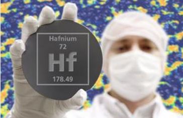
Note from the Nanoworld‹”Hafnium Oxide Helps Keep Microelectronics on the Moore¹s Law Trajectory”


Getting “Moore” By Using “Haf”

Hafnium oxide helps keep microelectronics on the Moore’s law trajectory

Read the article >

AFM vs. STM: The Resolution Battle

The uneasy truce has been broken, as AFM refuses to concede resolution superiority to STM.

Read the article >

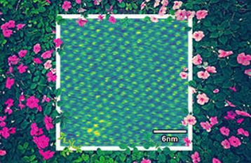
Springtime Beauty at the Nanoscale

Just like the brilliant blooms each spring, STM provides a captivating view of the world in which we live.

Read the article >

Note_Asyleum_3.JPG

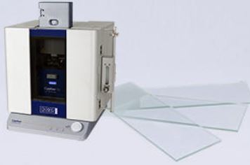
What’s Cypher’s High Resolution Secret?

You’ve seen Cypher’s high-resolution results, but what makes it possible? Roger Proksch shares the key secret to Cypher’s performance.

Read the article >

Note_Asyleum_4.JPG

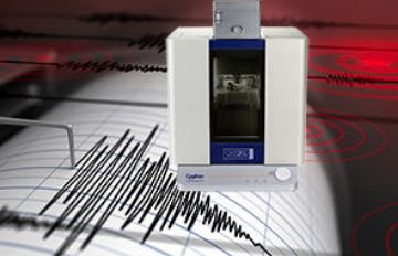
Cypher is a Terrible Earthquake Detector!

A man, a dog, and an AFM were sitting in a lab when an  earthquake hit. The AFM is the only one that wasn’t startled!

Read the article >

Note_Asyleum_5.JPG

Springtime Beauty at the Nanoscale

Just like the brilliant blooms each spring, STM provides a captivating view of the world in which we live.


Read the article >

Questions or Comments?

Save Big During Herzan’s – Summer Savings Program

Herzan_1

Herzan is excited to announce it’s Summer Savings Program! This program allows researchers to save big on Herzan’s most popular products (up to 30%), including the TS Series active vibration isolation tables, WaveCatcher site survey tools, and AEK-2002 acoustic enclosures.

Don’t delay, start saving for your research today!

Herzan_Summer_1

These promotions are available for a limited time: 9/30/2018. Click the links below to check out these exclusive offers!

Herzan_Summer_4.JPG

AEK-2002_2.JPG

New Asylum Research AFM Accessory Enables Advanced Magnetics Research Under Both In-Plane and Out-of-Plane Applied Magnetic Fields

July 24, 2018 (Santa Barbara, CA) Understanding and characterizing magnetic properties at the nanoscale is one of the key challenges in developing next-generation data storage and logic elements.  The new Variable Field Module (VFM4) accessory for Asylum Research MFP-3D Atomic Force Microscopes (AFMs) enables measurements under applied in-plane and out-of-plane magnetic fields in order to better understand their effects on nanoscale magnetic domain structure. The VFM4 is capable of applying either an adjustable in-plane (±8000 G ) or out-of-plane (±1200 G) magnetic field to a sample and offers ~1 G field resolution. Researchers can learn more about the VFM4 and see recent results at http://afm.oxinst.com/VFM4.

“This new combination of capabilities has allowed one customer at a national synchrotron facility to use AFM for research that was previously only possible with very costly and time-consuming scanning x-ray transmission microscopy (SXTM),” said Dr. Maarten Rutgers, Director of New Product Introduction. “No other AFM commercial solution offers the same capabilities, versatility, and ease of use for magnetics research. While the VFM has traditionally been used for magnetic force microscopy experiments, it can also be used with techniques like conductive AFM (CAFM) and on a wide range of diverse samples including piezoelectric and ferroelectric materials.”

The VFM4 easily attaches to most Asylum Research MFP-3D AFMs and includes replaceable pole tips to quickly adapt between in-plane and out-of-plane configurations. It maintains a steady magnetic field with rare-earth magnets that produce no heat, thermal drift, or mechanical vibration. For experiments where both an applied magnetic field and a high tip-sample voltage bias are required, there is an optional high-voltage kit to adapt the VFM4 for safe application of voltages up to ±220 Volts.

Image caption:  Magnetic skyrmions in Co-based thin film pads imaged with MFM under out-of-plane magnetic fields. Image courtesy of K. Bouzehouane, Unité Mixte de Physique CNRS, Thales, Univ. Paris-Sud, Université Paris-Saclay France.


Applied Magnetic Fields

        Download PDF

About Oxford Instruments Asylum Research

Oxford Instruments Asylum Research is the technology leader in atomic force microscopy for both materials and bioscience research. Asylum Research AFMs are widely used by both academic and industrial researchers for characterizing samples from diverse fields spanning material science, polymers, thin films, energy research, and biophysics. In addition to routine imaging of sample topography and roughness, Asylum Research AFMs also offer unmatched resolution and quantitative measurement capability for nanoelectrical, nanomechanical and electromechanical characterization. Recent advances have made these measurements far simpler and more automated for increased consistency and productivity.  Its Cypher™ and MFP-3D™ AFM product lines span a wide range of performance and budgets.  Asylum Research also offers its exclusive SurfRider™ AFM probes among a comprehensive selection of AFM probes, accessories, and consumables. Sales, applications and service offices are located in the United States, Germany, United Kingdom, Japan, France, India, China and Taiwan, with distributor offices in other global regions.

About Oxford Instruments plc 

Oxford Instruments designs, supplies and supports high-technology tools and systems with a focus on research and industrial applications. Innovation has been the driving force behind Oxford Instruments’ growth and success for over 50 years, and its strategy is to effect the successful commercialisation of these ideas by bringing them to market in a timely and customer-focused fashion.

The first technology business to be spun out from Oxford University, Oxford Instruments objective is to be the leading provider of new generation tools and systems for the research and industrial sectors with a focus on nanotechnology. Its key market sectors include nano-fabrication and nano-materials. The company’s strategy is to expand the business into the life sciences arena, where nanotechnology and biotechnology intersect.

This involves the combination of core technologies in areas such as low temperature, high magnetic field and ultra high vacuum environments; Nuclear Magnetic Resonance; x-ray, electron, laser and optical based metrology; atomic force microscopy; optical imaging; advanced growth, deposition and etching.

Oxford Instruments aims to pursue responsible development and deeper understanding of our world through science and technology. Its products, expertise, and ideas address global issues such as energy, environment, security and health.

For further information please Contact Us

AFM Characterization of Emerging Photovoltaics Webinar September 13, 2018 at 11:30am EDT

September 13, 2018
11:30am-12:30pm EDT 
(3:30-4:30pm UTC)

This free webinar, held in conjunction with the Materials Research Society (MRS), provides an overview of AFM applications for emerging photovoltaics including hybrid organic-inorganic perovskites and organic semiconductors.

• Discover the latest AFM techniques to accurately map local photocurrent, work function, and other electrical response in photoactive materials and charge transport layers

• See real-world results from leading researchers in the field on a variety of photovoltaic systems using standard and advanced AFM techniques

• Learn how AFM has become simpler with turnkey instrumentation for better AFM optical experim

Presenters

Dr. Rajiv Giridharagopal, Ginger Lab, University of Washington–Seattle

Rajiv Giridharagopal has been a Senior Research Scientist in Prof. David Ginger’s laboratory at the University of Washington–Seattle since 2015, with a research focus on SPM development for photovoltaic, bioelectronic, and related materials. He previously worked at the Intel Corporation in optical microscopy development. He earned a Ph.D. in Electrical Engineering from Rice University and holds two patents.

Dr. F. Ted Limpoco, Oxford Instruments Asylum Research

Ted Limpoco is an Applications Scientist at Oxford Instruments. He has over 10 years of AFM experience in nanoelectrical, nanomechanical, and nanotribology techniques. He was previously a postdoctoral fellow at the University of Illinois at Urbana-Champaign and has a Ph.D. in chemistry from the University of Florida.


Webinar Archives

  • Cypher VRS Video-Rate AFM
  • Graphene and 2D Materials
  • Choosing the Best AFM Probe
  • Analysis of Thin Films
  • Characterization of Polymers
  • Advanced PFM
  • Introduction to PFM
  • Cypher AFM
  • blueDrive Photothermal Excitation
  • Nanomechanical Mapping with Contact Resonance
  • Getting Started with AFM and Biology
  • Nanomechanical Mapping with AM-FM Mode
  • Ultra-High Resolution Imaging wih Cypher AFMs

Who Should Attend


Discover the latest innovations in environmental control at Herzan’s booth (Booth 1206) during the M&M Meeting 2018.


We at Herzan are excited to meet with researchers at the Microscopy & Microanalysis Meeting in the Baltimore Convention Center in Baltimore, Maryland.

We will be sharing our latest innovations in the field of environmental control, designed specifically to address needs within the microscopy community.

Stop by Booth 1206 to learn more about the unprecedented vibration isolation performance of the AVI Series and discover how you can save money and time installing an instrument by utilizing the WaveCatcher site survey tool.

Also, there will be some free giveaways at the booth to bring home to family and friends and share with colleagues in the lab! 

WHEN: Aug 5th – 9th, 2018
Exhibit Dates: Aug 6th – 9th, 2018

WHERE: Baltimore Convention Center, Baltimore, MD (Booth 1206)

WHAT: Discover Herzan’s Innovations for Environmental Control

Popular Applications

Herzan’s environmental solutions support a wide range of research applications relevant to M&M attendees, including:

Atomic Force Microscopy

Electron Microscopy

 Tribology

Interferometry