Author: Web Administrator

Press Release – Asylum Research Announces New Electrochemistry Cell

EC cell for AFM- electrochemical measurements of 2d materials

See it yourself

Now scheduling demos!


MRS Fall Meeting, booth #510
Nov 29-Dec 1 | Boston, MA
imageszzaf7sgu

Press Release

The Highest Performance Electrochemical AFM (EC-AFM)

The Cypher ES with EC Cell: See electrochemical reactions in real time. Compatible with a wide range of materials.

The Electrochemistry Cell for the Asylum Research Cypher ES atomic force microscope is the premier solution for in situ AFM characterization of electrochemical processes. Its simple modular design provides great versatility and compatibility with a wide range of materials. Best of all, it is based on the Cypher ES AFM— the world’s highest resolution, fast scanning AFM with superior environmental control and ease of use for maximum productivity.

  • Fully sealed EC cell with uniquely designed cantilever holder and liquid cup for easy imaging in fluid
  • Compatible with most common and cutting-edge electrolytes and electrode materials
  • Simple to clean and assemble, even with gloves
  • Optional heating and cooling stages allow investigation of electrochemical thermodynamics
  • Glovebox option provides the ultimate environmental control with no performance compromises

Voltammogram showing reductive deposition and oxidative stripping of copper

Time series of AFM images showing the electrochemical stripping of copper from a gold electrode in an acidic 0.1 M copper sulfate solution. Imaged in tapping mode using blueDrive photothermal excitation. Graph: Voltammogram showing reductive deposition and oxidative stripping corresponding to the process shown in the images above.

Applications for the EC Cell

Electrodeposition • Energy Storage • Corrosion

  • Characterizing energy storage materials under bias, such as battery electrodes, membranes and solution-electrode interfaces
  • Electrodeposition and stripping of metals
  • Investigating kinetics of corrosion
  • Monitoring morphology over time of electrode-attached biocatalysts, microorganisms, and other biophysical research
  • Nucleation and growth of nanoparticles

See it yourself

Extrusion On Just The Right Scale – Lab, Pilot, Small-Batch, Online Processing

Having trouble viewing this email? Click here.
Thermo Scientific
Thermo Fisher Scientific

Talk to an expert today and ask about special offers on extrusion systems.

contact


Optimize development of new polymer formulations with the Thermo Scientific™ Process 11 Parallel Twin-Screw Benchtop Extruder. We offer many extrusion solutions for novel materials.

The Process 11 parallel co-rotating extruder needs only a small amount of material (20 grams per hour) to conduct experiments, so you can run numerous trials with great efficiency. And it scales up to 2.5 kilograms of material per hour so you can easily mimic final production and conduct scale-up quickly and with confidence.

Customize the Process 11 extruder for your specific applications with a broad range of accessories such as the water bath, Pelletizer, or our new sheet die and chilled sheet take-off to help simulate full scale production.

Test specimen production
Create ISO/ASTM-compliant test specimens in process development after compounding tiny samples in the R&D lab with the Thermo Scientific™ HAAKE™ MiniJet Pro Injection Molding System. Ease the worries of limited material quantities and produce various sample geometries with the HAAKE MiniJet Pro Sample Preparation system.

You may also be interested in:

Featured application note:

Relevant Process Parameters for Upscaling in Twin-screw Compounding.

Key products video:

Small scale twin-screw compounding with the 11mm twin screw extruder, Process 11 extruder, combined with the HAAKE MiniJet laboratory injection molding system.

 Product literature:

Twin-screw extruders: Brochure for comprehensive compounding and extrusion solutions in materials science


Learn more about the Process 11 Extruder and HAAKE MiniJet Pro Injection Molding System.

 For Research Use Only. Not for use in diagnostic procedures.

src_logo_colour
5805 Kennedy Rd., Mississauga ON, L4Z 2G3 | TEL: 905 890 2010 – FAX: 905 890 1959
Integrys Limited, ACA TMetrix Inc. and Spectra Research Corp, are subsidiary companies of The ACA Group of Companies
Copyright © 2016 Spectra Research Corporation. All Rights Reserved.
Thermo Fisher Scientific

Webinar : Boost food development and processing workflows with rheology that drives results.

Boost food development and processing workflows with rheology that drives results.
Having trouble viewing this email? Click here.
Invitrogen by Thermo Fisher Scientific
Is your sample good enough? NanoDrop One has the answer.
Boost food development and processing workflows with rheology that drives results.

Watch Webinar

This webinar covers the basics of food rheology demonstrated with practical examples of real-world processes for critical food factors such as:

  • Mouthfeel, spreadability, processability
  • Time and temperature dependent behavior
  • Filling behavior and extensional rheology
  • Aggregation and disaggregation along with thixotropy

You can benefit from this webinar if you’re involved in the development, characterization or testing of food products and their processability.

Visit our Rheology of Food web page, or contact us about Thermo Scientific™ HAAKE™ MARS™ rheometers to spur your business forward.

FREE Half-day workshop dedicated to advances in Extrusion, Compouding and Rheology

workshop dedicated, advances Extrusion, Compouding and Rheology 
Thermo Scientific
Thermo Fisher Scientific
FREE Half-day workshop dedicated to advances in
Extrusion, Compounding, and Rheology

Get the most information from your material for QC and R&D, with Thermo Scientific™ extruders, compounders, rheometers, and viscometers, designed to accurately measure the properties of fluids and other complex materials.

Coverage includes:

  • Optimizing Material and Processes Through Rheological Measurements
  • Utilizing Small Scale Processing in Formulation and R&D
  • Implementing Scalable Extrusion Solutions from Development to Production
  • Gaining Molecular Level Analysis through Hyphenated Techniques
Register today

Wednesday,
October 5

Corporate Event Centre at CHSI
5110 Creekbank Rd.
Mississauga, ON

8:00a.m. – 2:00p.m.

Register today – space is limited
Learn more detailed information about the workshop sessions »
Workshop Dates & Locations
Wednesday, September 14, 2016 Fremont, CA
Wednesday, September 21, 2016 Houston, TX
Wednesday, September 28, 2016 Cleveland, OH
Wednesday, October 05, 2016 Mississauga, ON, CA
Tuesday, October 18, 2016 Columbia, MD
Thursday, October 20, 2016 Plainsboro, NJ

Agenda
8:00-8:45 Registration and Continental Breakfast
8:45-9:00 Opening Remarks
9:00-9:45 Optimizing Material and Processes Through Rheological Measurements
9:45-10:45 Utilizing Small Scale Processing in Formulation and R&D
10:45-11:00 Coffee Break
11:00-11:30 Scalable Extrusion Solutions – From Development to Production
11:30-12:15 Gaining Molecular Level Analysis through Hyphenated Techniques
12:15-1:00 Lunch
1:00-2:00 Live Demonstration
Your privacy is important to us. View our Privacy Policy. 168 Third Avenue, Waltham, MA 02451 USA © 2016 Thermo Fisher Scientific Inc. All Rights Reserved.

Asylum Research Presents AFM Probe Webinar

Oxford Instruments Asylum Research Presents the Webinar “How to Choose the Right Probe for Your Atomic Force Microscopy Experiments”

Target audience: All AFM users

Keywords: Atomic Force Microscopy (AFM), Scanning Probe Microscopy (SPM), probes, cantilever

August 24, 2016 (Santa Barbara, CA) Successful atomic force microscopy (AFM) imaging starts with choosing the right probe for your sample and scan mode. It’s one of the most important considerations when doing an experiment. Asylum Research’s webinar “How to Choose the Right Probe for Your AFM Experiments” aims to make all AFM users experts at probe selection. The webinar will be presented September 8, 2016, 8:00am PDT, by Asylum Research Applications Scientist, Dr. Ted Limpoco. Registration is at www.oxford-instruments.com/ProbeWebinar.

“Choosing the right probe from hundreds available, even for an experienced user, can be a daunting task,” said Dr. Limpoco. “At Asylum, we scan an incredible number of different samples under various conditions and modes daily, so we have a deep understanding of what works and what doesn’t. This is an excellent opportunity to share our knowledge and experience with the entire AFM community.”

Topics discussed in the webinar include:
• AFM probe fundamentals and calibration
• Probe selection for imaging in air and liquid
• Probe selection for specific scan modes (e.g. MFM, high resolution imaging, nanomechanics)
• Specialized probes
• Real-world image examples

About Oxford Instruments Asylum Research

Oxford Instruments Asylum Research is the technology leader in atomic force microscopy for both materials and bioscience research. Asylum Research AFMs are widely used by both academic and industrial researchers for characterizing samples from diverse fields spanning material science, polymers, thin films, energy research, and biophysics.

In addition to routine imaging of sample topography and roughness, Asylum Research AFMs also offer unmatched resolution and quantitative measurement capability for nanoelectrical, nanomechanical and electromechanical characterization.

Recent advances have made these measurements far simpler and more automated for increased consistency and productivity. Its Cypher™ and MFP-3D™ AFM product lines span a wide range of performance and budgets. Asylum Research also offers its exclusive SurfRider™ AFM probes among a comprehensive selection of AFM probes, accessories, and consumables. Sales, applications and service offices are located in the United States, Germany, United Kingdom, Japan, France, India, China and Taiwan, with distributor offices in other global regions.

About Oxford Instruments plc

Oxford Instruments designs, supplies and supports high-technology tools and systems with a focus on research and industrial applications. Innovation has been the driving force behind Oxford Instruments’ growth and success for over 50 years, and its strategy is to effect the successful commercialisation of these ideas by bringing them to market in a timely and customer-focused fashion.

The first technology business to be spun out from Oxford University, Oxford Instruments objective is to be the leading provider of new generation tools and systems for the research and industrial sectors with a focus on nanotechnology. Its key market sectors include nano-fabrication and nano-materials. The company’s strategy is to expand the business into the life sciences arena, where nanotechnology and biotechnology intersect.

This involves the combination of core technologies in areas such as low temperature, high magnetic field and ultra high vacuum environments; Nuclear Magnetic Resonance; x-ray, electron, laser and optical based metrology; atomic force microscopy; optical imaging; advanced growth, deposition and etching.

Oxford Instruments aims to pursue responsible development and deeper understanding of our world through science and technology. Its products, expertise, and ideas address global issues such as energy, environment, security and health.

For further information please Contact Us

Applications of the NanoRack™ Sample Stretching Stage to a Commercial Impact Copolymer

Dalia G. Yablon and Andy H. Tsou, ExxonMobil Research and Engineering, Clinton, NJ

A commercial impact copolymer (ICP), amulticomponent material typically used inautomotive and appliance applications where a balance of stiffness and toughness is needed, was studied with the NanoRack™ Sample Stretching Stage accessory on the MFP-3D™Atomic Force Microscope to investigate material deformation and interface adhesion as a function of tensile stress. Effects of deformation were observed within both the polypropylene  and ethylene-propylene components, as well as at the interface between the two materials. There are no other direct measurement methods available to determine interfacial adhesive strength of polymer blends, and so AFM investigations of micro-domain deformation such as the one described here could be used ultimately to provide a direct determination of interfacial adhesion in complex polymer containing materials such as ICP. Studies of this kind improve our understanding of material structure-propertyrelationships, ultimately enabling manufacture of better quality products.

Application to Impact Copolymer (ICP)

The commercial impact copolymer used for this study is composed of a polypropylene (PP) matrix with micron-sized domains of ethylene-propylene (EP) rubber domains produced in a serial polymerization reactor. Dogbone-shaped samples were molded of the impact copolymer measuring at ~20mm (middle straight part of dogbone) by ~4mm in width by 0.2mm thickness. A portion of the straight part of the dogbone was cryo-faced at -120°C with a cryomicrotome to ensure a smooth sample and to remove the thin polymer

   CopolymerStretchingANLR-1

Figure 1: Stress (Newtons) vs. time (seconds) curve of ICP as it is being stretched on the NanoRack.

surface layer that forms during the compression molding process (also referred to as a ‘polymer skin’), leaving a small and smooth surface area in the middle of the dogbone that was suitable for imaging. The sample was mounted into a NanoRack Sample Stretching Stage with smooth grips. The NanoRack is a high-strain, high-travel manual stretching stage that provides two-axis stress control of tensile loaded samples and also allows control of the sample image region under different loads. Automatic load cell calibration provides integrated force measurements with MFP-3D images or other measurements and returns both stress and strain data.

Figure 1 shows real-time stress vs. time curves of the ICP as the sample is being pulled in the NanoRack. The baseline force is

download

AFM Characterization of Thin Films: High-Resolution Topography and Functional Properties

Asylum Research Cypher™ and MFP-3D™ atomic force microscopes (AFMs) provide valuable information for characterizing thin films and coatings. They quantify 3D roughness and texture with unmatched spatial resolution and measure nanoscale functionality including electrical, magnetic, and mechanical behavior.

Thin films and coatings play a critical role in everything from food containers to photovoltaics. To meet such varied needs, they are made from every class of material and by numerous processes including physical and chemical vapor deposition techniques, atomic layer deposition, and sol gel processing.A key step in developing any new film is characterizing its surface structure and physical properties, whether in engineering commercial products (Figure 1) or pursuing fundamental materials science (Figure 2).

The intrinsic dimensions of films (thickness, grain and domain sizes, etc.) make it important to characterize them on sub-nanometer to micrometer length scales. The AFM is a powerful tool for this purpose for many reasons. For instance, it possesses much higher spatial resolution than other stylus or optical-based methods.4 Samples need not be optically reflective or electrically conducting, allowing access to virtually any film. AFMs also provide complementary information to electron microscopes, such as accurate 3D surface profiles, and offer a more flexible operating environment for work at both ambient and non-ambient atmospheres and temperatures.

Here we describe the extensive features of Asylum Research AFMs for thin film characterization and show examples over a range of applications. With today’s AFMs, surface roughness can be measured more accurately, quickly, and easily than ever before. A wider array of built-in analysis tools and automated routines mean higher productivity and greater ease of use. Also, research and instrumentation advances have created a variety of AFM modes for measuring nanoscale film functionality including electrical, magnetic, and mechanical response.

Thin-Films-Characterization-AFM-2

Thin-Films-Characterization-AFM-1
Figure 2: Strain effects in ferroelectric NaNbO3 (NNO) films grownon TbScO3 (TSO) substrates with metal organic chemical vapordeposition (MOCVD). Growth of epitaxial NNO on TSO results in significant anisotropic misfit strain. Understanding relations between strain, crystal structure, and ferroelectric response will enable finetuning

of film properties. The lateral piezoresponse force microscopy (PFM) image on a film with thickness d=11 nm reveals a strong in-plane piezoresponse with highly ordered domains (vertical stripes).
For a thicker film (d=21 nm), distortions in the alignment appear. For an even thicker film (d=66 nm), 90º domains (horizontally striped regions) are observed, indicating a 1D to 2D domain pattern transformation. The graph shows values for the lateral piezoelectric domain width D obtained by PFM and x-ray diffraction (XRD). The dependence of D on d changes from approximately constant to the predicted D∝d 0.5 (dotted line) at d≈20 nm, where the 1D
to 2D transformation occurs. Acquired on the MFP-3D AFM. Adapted from Ref. 3.
Figure 1: Oxygen plasma treatment of polyethylene terephthalate(PET) films. PET fibers coated with a conducting polymer such as polypyrrole could be used in “smart” electronic textiles. However, achieving good coating-to-fiber adhesion remains a key challenge.Images of PET films exposed to oxygen plasma show that RMS surface roughness increased with exposure time. Films processed longer than 60 s displayed surface etching and uniform nanoscale features. The graph reveals a linear dependence of roughness on treatment time after ~30 s. Combined with data on surface chemistry, the results can be used to optimize treatment parameters for improved coating adhesion and conductivity. Scan size 1 μm; height scale 35 nm. Imaged with the Cypher S AFM. Adapted from Ref. 2. AFM Characterization-Thin Films
download

New Application Note Describes Atomic Force Microscopy Tools for Nanoscale Electrical Characterization

Oxford Instruments Asylum Research announces its new application note describing atomic force microscopy (AFM) tools for nanoelectrical characterization. The application note discusses the most recent nanoelectrical characterization techniques, as well as the benefits and exclusive modes that the Asylum Research Cypher™ and MFP-3D™ AFMs offer. Researchers will learn more about evaluating local electrical properties, including current, surface charge and potential, dielectric breakdown, conductivity, and permittivity.

The application note can be downloaded at www.oxford-instruments.com/electrical-characterization.

Not only do the dimensions of silicon-based devices keep shrinking to a few nanometers, but also next- generation processes with nanoscale components like nanotubes, graphene, and molecular building blocks are emerging. Understanding physical processes that control electrical behavior increasingly

requires AFM measurements on smaller length scales,” said Keith Jones, Asylum Research Applications Scientist, specializing in electrical characterization. “This application note is a great reference for scientists new to AFM as well as those currently working in the field.”

Asylum Research AFMs are being used by leading researchers around the globe for characterizing nanoelectrical properties. A variety of their publications can be found at: www.oxford-instruments.com/nanoelectrical-afm.

Figure caption: Kelvin Probe Force Microscopy surface potential overlaid on topography for flakes of boron nitride (small triangles) and graphene (large irregular features) grown on a copper foil substrate.

About Oxford Instruments Asylum Research

Oxford Instruments Asylum Research is the technology leader in atomic force microscopy for both materials and bioscience research. Asylum Research AFMs are widely used by both academic and industrial researchers for characterizing samples from diverse fields spanning material science, polymers, thin films, energy research, and biophysics. In addition to routine imaging of sample topography and roughness, Asylum Research AFMs also offer unmatched resolution and quantitative measurement capability for nanoelectrical, nanomechanical and electromechanical characterization. Recent advances have made these measurements far simpler and more automated for increased consistency and productivity.  Its Cypher™ and MFP-3D™ AFM product lines span a wide range of performance and budgets.  Asylum Research also offers its exclusive SurfRider™ AFM probes among a comprehensive selection of AFM probes, accessories, and consumables. Sales, applications and service offices are located in the United States, Germany, United Kingdom, Japan, France, India, China and Taiwan, with distributor offices in other global regions.

About Oxford Instruments plc

Oxford Instruments designs, supplies and supports high-technology tools and systems with a focus on research and industrial applications. Innovation has been the driving force behind Oxford Instruments’ growth and success for over 50 years, and its strategy is to effect the successful commercialisation of these ideas by bringing them to market in a timely and customer-focused fashion.

The first technology business to be spun out from Oxford University, Oxford Instruments objective is to be the leading provider of new generation tools and systems for the research and industrial sectors with a focus on nanotechnology. Its key market sectors include nano-fabrication and nano-materials. The company’s strategy is to expand the business into the life sciences arena, where nanotechnology and biotechnology intersect.

This involves the combination of core technologies in areas such as low temperature, high magnetic field and ultra high vacuum environments; Nuclear Magnetic Resonance; x-ray, electron, laser and optical based metrology; atomic force microscopy; optical imaging; advanced growth, deposition and etching.

Oxford Instruments aims to pursue responsible development and deeper understanding of our world through science and technology. Its products, expertise, and ideas address global issues such as energy, environment, security and health.

Correlative Raman imaging: New insights for bio-mineral and nano materials

AFM topography (top) and Raman (bottom) images of the cuticle of a Crustacea. The Raman image reveals the distribution of amorphous Calcium carbonate phases (red & blue) along with additional organic compounds (green).
Correlative Raman imaging: New insights for bio-mineral and nano materials

Watch this on-demand free webinar by Logging In or Signing Up below.

In nature, biomineralization is a widespread and evolutionarily ancient phenomenon. It’s the molecular basis for the formation of pearls, bones, exoskeletons of crustaceans, teeth, molluscan shells, kidney stones and many other biological structures. To build structural features organisms from bacteria to humans use many varieties of minerals such as hydroxyapatite, calcium carbonates and phosphate, silica and magnetite.

Raman Imaging in combination with Atomic Force Microscopy (AFM) or Scanning Electron Microscopy (SEM) can provide new insights into the fundamental processes by which organisms produce biocomposites containing crystallized minerals. After an understanding of the mechanisms of biomineralization is obtained, it should be possible to  exploit them in technical applications.

In this webinar we will first introduce the principles of state-of-the-art confocal Raman imaging as a tool for analyzing the chemical and molecular characteristics of a sample.

Then we will show how this technique can be used in combination with AFM and SEM to correlate  chemical information with structural features. Altogether it will demonstrate the advantages  of microscopy systems that integrate Raman-AFM and Raman-SEM (RISE), respectively, in standalone hybrid instruments.

  • Hear from a leading manufacturer of confocal Raman microscopes how to perform Raman imaging and interprete Raman data.
  • Understand the remarkable potential of correlative Raman-AFM and Raman-SEM approaches using “all-in-one” instrumental setups for investigating complex organic materials.
  • Learn about the application of Raman imaging for the characterization of mineralized structures of organisms.

Speakers:

Dr. Ute Schmidt, Applications Manager at WITec GmbH
Joe D’angelo, (Moderator), Materials Science Publisher.

Already a Materials Today member?

Log in to your Materials Today account to access this webinar.

Share this webinar…

Join the conversation…
Most viewed in nanomaterials…

Webinar

18 Aug ’16

Chemistry in the TEM – New Horizons for Catalyst Research

News

Improve Productivity with the new QC Rheometer

Having trouble viewing this email? Click here.
Invitrogen by Thermo Fisher Scientific
Viscotester iQ Air Rheometer
Extend your capabilities of measurement range

Are you interested in testing water-like materials in rotational mode?
– See the advantages in –

Testing low viscosity
fluids with the HAAKE Viscotester iQ Air

Are you performing oscillatory tests on
visco-elastic fluids?
– Read more about –

Performing enhanced rheological tests in oscillation with the HAAKE Viscotester iQ Air

Are you conducting
creep and recovery tests on complex fluids
or semi solids?
– Discover –

Creep and recovery tests of cosmetic emulsion performed with the HAAKE Viscotester iQ Air

Increase your workflow efficiency and benefit from intelligent user guidance. Discover the six reasons why today!
Download PDF
Ready to talk to us about your needs? Contact us today!
 Thermo Fisher Scientific


The NanomechPro ™ Toolkit:

Accurate Tools for Measuring Nanoscale Mechanical Properties for Diverse Materials

Understanding nanoscale mechanical properties is of fundamental importance for evaluating the behavior and performance of a wide NanomechProDSHR-1
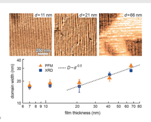
variety of industrially, biologically and structurally important materials. An Atomic Force Microscope (AFM) tip interacting with a sample experiences forces originating from many different sources – elasticity, viscosity, adhesion, van der Waals – to name a few. Hence, it has become increasingly clear that reliable and accurate materials properties measurements require looking at your sample in more than one way. Single techniques are simply insufficient for accurately and rigorously revealing sample properties and can often yield misleading and even inaccurate results and conclusions.

The NanomechPro™ toolkit (Figure 1) for Asylum’s Cypher™ and MFP-3D™ AFMs provides a suite of tools to meet the requirements of the nanomechanics researcher and is both impressively powerful and rapidly expanding. The various tools are complementary – each technique probes and records different responses of your samples – and often can be used  imultaneously (e.g. Figures 2a – d). Additionally, with the Cypher AFM, many of these new techniques can be combined with small, fast, low noise cantilevers, enabling measurements at noise levels and speeds previously impossible.

Combined Loss Tangent and AM-FM Imaging

Amplitude-modulated (AM) atomic force microscopy, also known as tapping mode or AC mode, is a proven, reliable and gentle imaging method with widespread applications. Previously, the contrast in tapping mode has been difficult to quantify. However, in this work we introduce two new techniques that allow unambiguous interpretation of material properties in tapping mode: AM-FM and Loss Tangent. Because these measurements are made simultaneously, there is a built-in check for self-consistency in the measurements. The new AM-FM imaging technique combines the features and benefits of normal tapping mode with the quantitative, high sensitivity of Frequency Modulation (FM) mode. Both Loss Tangent and AM-FM imaging can be performed simultaneously at high data acquisition rates. These techniques are exclusively available from Asylum Research, US patents 8,024,963, 7,937,991, 7,603,891, 7,921,466 and 7,958,563 with others pending.

download