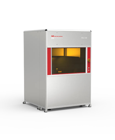
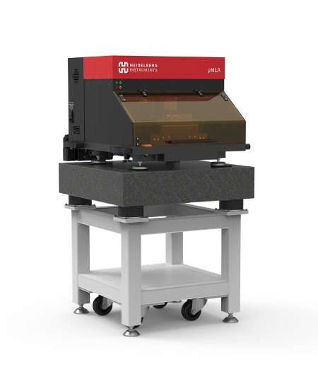
Description
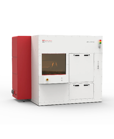
The µMLA (Micro Maskless Aligner) is an advanced tabletop lithography system designed for high-precision microstructuring and rapid prototyping. Built on the industry-leading µPG platform, it provides maskless direct-write lithography, eliminating mask-related costs and complexities. Ideal for research labs, MEMS development, microfluidics, micro-optics, and sensor fabrication, the µMLA enables high-resolution patterning with flexible exposure modes.
- Maskless Lithography: Eliminates mask-related expenses and security risks, offering direct-write lithography for R&D and prototyping.
- Dual Exposure Modes:
- Raster Scan Mode (Standard): Fast exposure with consistent write speeds regardless of pattern density.
- Vector Scan Mode (Optional): Optimized for smooth curved structures, such as waveguides and micro-optics.
- Variable Resolution Options: Choose from three optical setups for an optimal balance of throughput and resolution.
- Compact & Efficient: Smallest tabletop maskless aligner, fits on a standard workbench.
- Grayscale Lithography (Standard): Supports 2.5D structuring with up to 256 gray levels for micro-optics applications.
- User-Friendly Design: Features intuitive software, plug-and-play installation, and simplified sample handling.
Why Choose µMLA Maskless Lithography System?
- Fast & Cost-Effective: No masks are required, reducing costs and enabling rapid prototyping.
- Optimized for Diverse Applications: Ideal for microfluidics, MEMS, micro-optics, and semiconductor research.
- Customizable Exposure Settings: Flexible resolution and exposure mode choices for tailored fabrication needs.
- Grayscale Lithography for 2.5D Structuring: Supports complex micro-optics and microlens array designs.
- Plug-and-Play Installation: Intuitive setup and operation for quick integration into research labs.
- Upgradable & Scalable: Expandable exposure area and wavelength options for future needs.
Available Modules & Upgrades:
Exposure Modes:
- Raster Scan Exposure Mode (Standard): Fast, high-quality image writing, LED light source (365 nm or 390 nm).
- Vector Scan Exposure Mode (Optional): Smooth, continuous patterning for waveguides, Laser light source (405 nm and/or 375 nm).
Optical Configurations:
- Min. resolution of 0.6 µm, 1 µm, and 3 µm, with variable resolution choices.
- Multiple spot sizes available for vector exposure mode (0.6 µm to 50 µm).
Additional Features:
- Optional Overview Camera: Quick identification of alignment marks and substrate features.
- Draw Mode: Real-time drawing and overlaying of BMP files for custom microstructuring.
- Optical Autofocus: Ensures perfect exposure of small samples (<10 mm).
- Glovebox Integration: Patterning under controlled nitrogen environments.
- Customizable Exposure Area: Upgradable from 100 mm² to 150 mm².
Click here to view more products from Heildelberg Instruments.
FAQs (Frequently Asked Questions):
What applications is the µMLA best suited for?
The µMLA is ideal for R&D, MEMS, microfluidics, micro-optics, semiconductor prototyping, and rapid small-scale mask writing.
How does the Raster Scan Mode compare to Vector Scan Mode?
Raster Scan Mode provides fast, consistent exposure for various structure sizes. Vector Scan Mode is optimized for smooth, curved patterns, such as waveguides and diffractive optics.
Does this system support grayscale lithography?
Yes! The µMLA comes with grayscale exposure capability as a standard feature, supporting 2.5D structuring for micro-optics.
Can the µMLA be used for different wavelengths?
Yes! The Raster Scan Mode uses an LED light source (365 nm or 390 nm), while the Vector Scan Mode operates with a laser (405 nm and/or 375 nm).
What is the maximum exposure area?
The default exposure area is 100 x 100 mm² but can be upgraded to 150 x 150 mm².
How long does it take to expose a 4” wafer?
Approximately 90 minutes.
Is a cleanroom required for installation?
ISO 5 cleanroom conditions are recommended but not strictly required.