Description
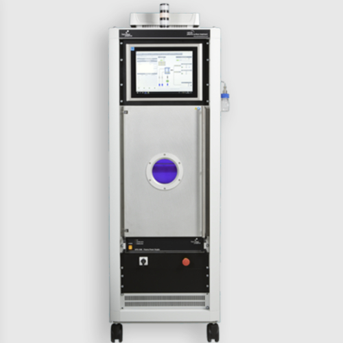
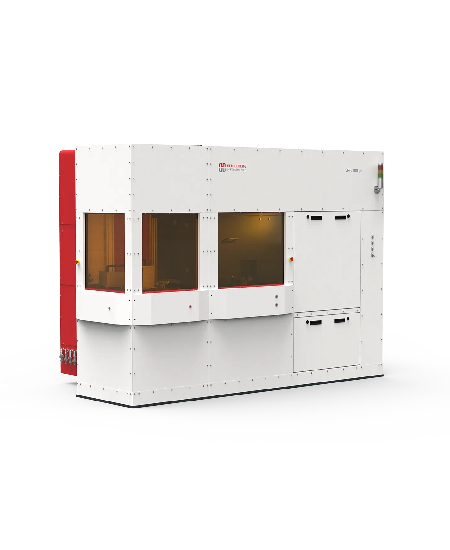
The DWL 66+ is a high-resolution direct-write laser lithography system designed for cutting-edge research, rapid prototyping, and mask-making applications. This versatile tool is ideal for microelectronics, MEMS, microfluidics, sensors, advanced packaging, and materials science.
With six configurable write modes, a choice of laser wavelengths (375 nm & 405 nm), and an extensive selection of modules, the DWL 66+ ensures unmatched precision, speed, and flexibility. It features grayscale lithography, enabling 2.5D microstructure fabrication for optical elements, holograms, and micro-optics.
Why Choose DWL 66+ High-Resolution Laser Lithography?
- Ultimate Versatility: Ideal for MEMS, photonics, semiconductor research, and microfabrication applications.
- Industry-Leading Resolution: 300 nm minimum feature size with 60 nm CD uniformity.
- Maskless, Direct-Write Lithography: Reduces turnaround time & eliminates mask-related costs.
- Advanced 2.5D Lithography Capabilities: Grayscale exposure for micro-optics and diffractive structures.
- Customizable & Scalable: Upgradable write modes, automation options, and substrate handling flexibility.
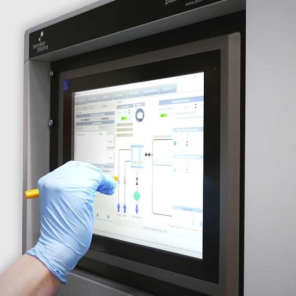
- Automated Workflow for Efficiency: Pre-aligners, wafer scanners, and automated mask handling for streamlined processing.
Click here to view more products from Heildelberg Instruments.
FAQs (Frequently Asked Questions):
What applications is the DWL 66+ best suited for?
The DWL 66+ is optimized for nanofabrication, MEMS, microfluidics, photonics, and semiconductor research.
What is the smallest feature size the DWL 66+ can pattern?
The system achieves minimum feature sizes of 300 nm in High-Resolution Mode.
How does grayscale lithography work on the DWL 66+?
It allows 2.5D structuring by exposing gradual intensity variations, creating topographies for micro-optics and holograms.
What are the main advantages of direct-write lithography?
No photomasks required, reducing costs, production time, and enabling rapid design iterations.
How does the automatic loading system improve efficiency?
It streamlines mask & wafer handling, reducing manual errors and improving throughput.
What are the benefits of the High-Accuracy Coordinate System?
Improves thermal stability, positioning accuracy, and 2nd layer alignment down to 350 nm.