Discount Products: Look through products available for a 25% – 50% discount in 2020. The items provided on a first come, first serve basis. View Discounted Products
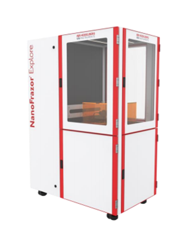
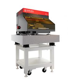
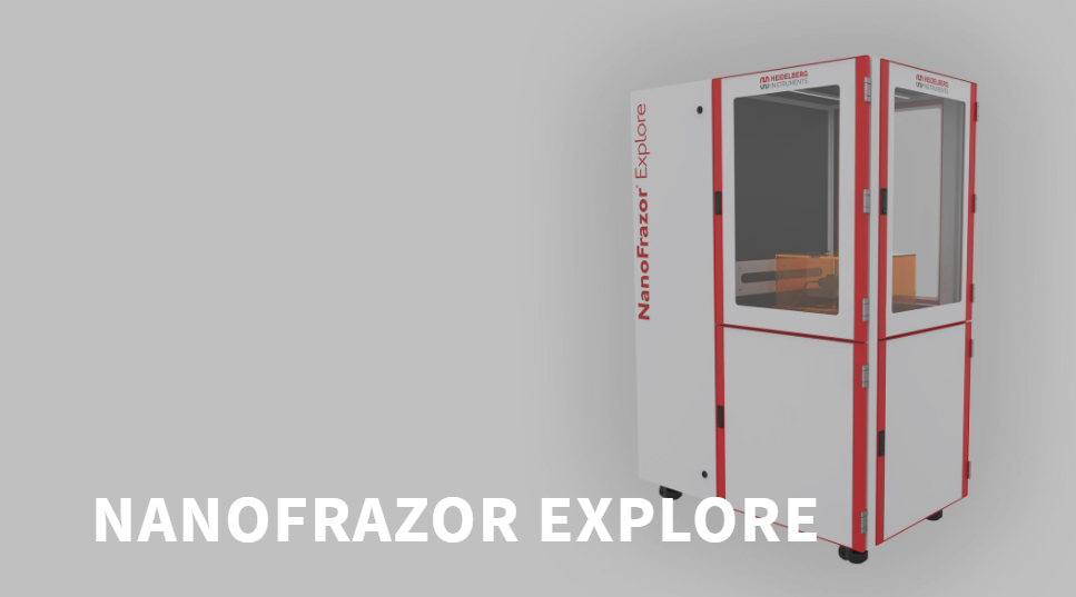
Introducing the Heidelberg Instruments NanoFrazor Explore
NanoFrazor Explore is the first commercial thermal scanning probe lithography tool. NanoFrazor Explore is used for nanopatterning of quantum devices on 1D/2D materials, such as quantum dots, Dolan bridges and Josephson junctions, and nanoscale arrays. Its unique capabilities enable new devices in new materials. For example, it is used for advanced applications such as grayscale photonics devices, nanofluidics structures or biomimetic substrates for cell growth; local modification of materials by heat, e.g. chemical reactions and physical phase changes.
The technology behind the system is the result of more than 20 years of intensive research and development (R&D) that started at IBM Research Zürich, and now happens at Heidelberg Instruments Nano. The NanoFrazor hardware and software are constantly advancing to extend the capabilities and performance of the tool and its range of applications. Our dedicated team of experts keeps developing and optimizing the pattern transfer processes for different applications. We compile this know-how in a growing collection of best practices and protocols to support our customers.
Key Features
High-resolution
Easy patterning of nanostructures even with complex geometries; min. lateral features 15 nm, Vertical resolution 2 nm
Thermal Scanning Probe Lithography
New approach to nanopatterning enabling applications not otherwise feasible
Non-invasive Lithography
No damage from charged particles, no proximity effects, clean lift-off
Compatibility
With all standard pattern transfer methods: lift-off, etching, etc – knowledge resource and best practices available in our “Recipe Book”
In-situ Imaging
Immediate control of patterned structures
Precise Overlay and Stitching
Markerless overlay and stitching accuracy 25 nm specified, sub-10 nm overlay shown
Unique Thermal Cantilevers
Integrated microheater and distance sensor; easy to exchange and economica
Laser Sublimation Module
High-throughput exposure of coarse structures in the same exposure step; 405 nm wavelength CW fiber laser
Compact
1.85 m x 0.78 m x 1.28 m
Vibration Isolation
Three-layer acoustic and superior vibration isolation (> 98% @ 10 Hz)
Low Cost of Ownership
No need for cleanroom, vacuum pump or expensive consumables
Key Benefits
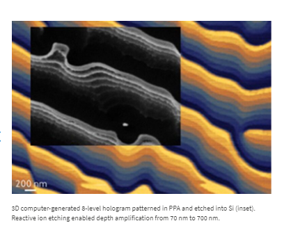
With the direct laser sublimation module, nano- and microstructures are now seamlessly and quickly written into the same resist layer in a single fabrication step. In-situ imaging enables two unique features: markerless overlay, and comparison of the written and target patterns during writing, so the parameters can be immediately adjusted. This approach, called closed-loop lithography, results in sub-2 nm vertical precision for 2.5D (grayscale) shapes of any complexity. Fast and precise control of a heated nanoscale tip enables innovation not otherwise feasible.
Grayscale Software Module
3D patterning at <2 nm vertical resolution
Decapede Module
10-tip write head for 10-fold increase in throughput fo high-resolution patterning
Glovebox Integration
Customized solution in collaboration with MBraun ensures minimized vibrations for work in controlled environments
Trust the Experts at Spectra Research Corporation
Spectra Research Corporation (SRC) offers a range of innovative high-quality scientific products and laboratory services to industrial and scientific markets throughout Canada.


