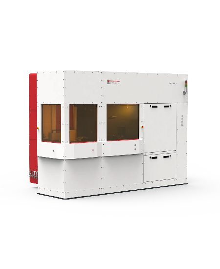
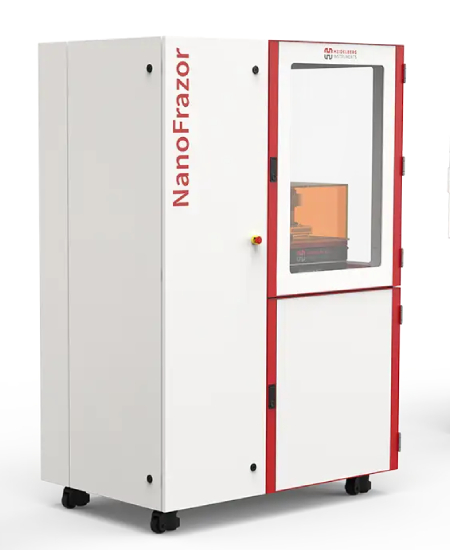
Description
The NanoFrazor is an innovative nanolithography system designed for thermal scanning probe lithography (t-SPL), enabling precise and damage-free patterning at the nanoscale. With its modular design, real-time in-situ imaging, and markerless overlay, the NanoFrazor Thermal Scanning Probe Lithography System offers unparalleled resolution, versatility, and automation for quantum devices, 2D materials, photonics, MEMS, and biotechnology applications.
This tool revolutionizes direct-write nanofabrication with Closed-Loop Lithography (CLL), ensuring sub-2 nm vertical precision, and integrates Direct Laser Sublimation (DLS) for high-speed patterning. Whether creating nano-optics, quantum dots, or biomimetic structures, the NanoFrazor provides ultimate flexibility for advanced research and industrial R&D.
Available Modules & Upgrades:
Direct Laser Sublimation (DLS) Module:
- High-throughput exposure of larger features (405 nm laser).
- Seamless integration with t-SPL for hybrid lithography.
Decapede Parallel Writing:
- 10 heated probe tips for faster nanoscale lithography.
- Independent parallel patterning with full precision.
Standalone Housing & Environmental Control:
- Three-layer acoustic isolation & vibration control.
- Integrated temperature, humidity, and gas-flow monitoring.
Glovebox Integration for Sensitive Materials:
- Nanopatterning inside a controlled environment.
Grayscale Software Module:
- 2.5D topography patterning with sub-2 nm depth resolution.
- Optimized for photonics, microfluidics, and biomimetic structures.
Automated Overlay & Stitching Software:
- Markerless alignment with real-time in-situ imaging.
- Improves accuracy and reduces patterning errors.
Dynamic Local Temperature Modulation:
- Enable heat-driven chemical reactions & phase changes.
- Ideal for advanced materials research
Why Choose NanoFrazor Thermal Scanning Probe Lithography System?
- Ultimate Nanolithography Precision: Sub-2 nm vertical and 15 nm lateral resolution.
- No Charged Particle Damage: Ideal for ultra-sensitive materials and devices.
- Real-Time In-Situ Imaging & Overlay: Immediate pattern validation and correction.
- Parallel Writing with Decapede Module: 10 simultaneous heated probes for large-area processing.
- Hybrid t-SPL & DLS Capabilities: Combining speed and resolution for complete device fabrication.
- Customizable & Scalable: Upgradable with additional modules and process optimizations.
- Grayscale Nanolithography: Precise depth control for photonics, optics, and biomimetics.
Click here to view more products from Heildelberg Instruments.
FAQs (Frequently Asked Questions):
What applications is the NanoFrazor best suited for?
Quantum devices, 2D materials, micro-optics, photonics, nanofluidics, and MEMS/NEMS fabrication.
What makes NanoFrazor unique compared to other lithography tools?
Thermal Scanning Probe Lithography (t-SPL) enables ultra-high resolution without charged particle damage or proximity effects.
What is the smallest feature size the NanoFrazor can achieve?
The NanoFrazor achieves 15 nm lateral resolution and sub-2 nm vertical resolution.
Does the NanoFrazor support grayscale lithography?
Yes! 2.5D patterning with <2 nm vertical accuracy is standard for optical, biomedical, and semiconductor applications.
What are the benefits of Direct Laser Sublimation (DLS)?
Faster exposure of coarse features (≥600 nm) using a 405 nm laser.
Can the NanoFrazor be integrated into a glovebox?
Yes! A full glovebox integration option is available for sensitive nanomaterial research.